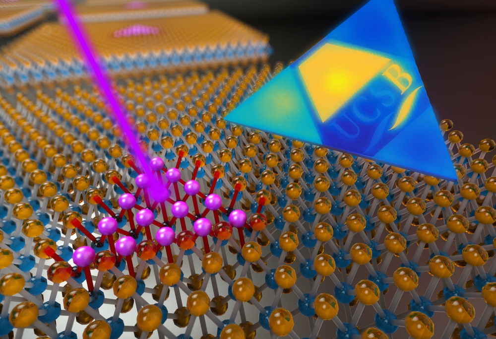
This artist’s representation shows an electron beam (in purple) being used to create a 2D superlattice made up of quantum dots having extraordinary atomic-scale precision and placement.
Control is a constant challenge for materials scientists, who are always seeking the perfect material — and the perfect way of treating it — to induce exactly the right electronic or optical activity required for a given application.
One key challenge to modulating activity in a semiconductor is controlling its band gap. When a material is excited with energy, say, a light pulse, the wider its band gap, the shorter the wavelength of the light it emits. The narrower the band gap, the longer the wavelength.
As electronics and the devices that incorporate them — smartphones, laptops and the like — have become smaller and smaller, the semiconductor transistors that power them have shrunk to the point of being not much larger than an atom. They can’t get much smaller. To overcome this limitation, researchers are seeking ways to harness the unique characteristics of nanoscale atomic cluster arrays — known as quantum dot superlattices — for building next generation electronics such as large-scale quantum information systems. In the quantum realm, precision is even more important.
New research conducted by UC Santa Barbara’s Department of Electrical and Computer Engineering reveals a major advance in precision superlattices materials. The findings by Professor Kaustav Banerjee, his Ph.D. students Xuejun Xie, Jiahao Kang, and Wei Cao, postdoctoral fellow Jae Hwan Chu and collaborators at Rice University appear in the journal Nature Scientific Reports.
Their team’s research uses a focused electron beam to fabricate a large-scale quantum dot superlattice on which each quantum dot has a specific pre-determined size positioned at a precise location on an atomically thin sheet of two-dimensional (2-D) semiconductor molybdenum disulphide (MoS2). When the focused electron beam interacts with the MoS2 monolayer, it turns that area — which is on the order of a nanometer in diameter — from semiconducting to metallic. The quantum dots can be placed less than four nanometers apart, so that they become an artificial crystal — essentially a new 2-D material where the band gap can be specified to order, from 1.8 to 1.4 electron volts (eV).
This is the first time that scientists have created a large-area 2-D superlattice — nanoscale atomic clusters in an ordered grid — on an atomically thin material on which both the size and location of quantum dots are precisely controlled. The process not only creates several quantum dots, but can also be applied directly to large-scale fabrication of 2-D quantum dot superlattices. “We can, therefore, change the overall properties of the 2-D crystal,” Banerjee says.
Each quantum dot acts as a quantum well, where electron-hole activity occurs, and all of the dots in the grid are close enough to each other to ensure interactions. The researchers can vary the spacing and size of the dots to vary the band gap, which determines the wavelength of light it emits.
“Using this technique, we can engineer the band gap to match the application,” Banerjee says. Quantum dot superlattices have been widely investigated for creating materials with tunable band gaps but all were made using “bottom-up” methods in which atoms naturally and spontaneously combine to form a macro-object. But those methods make it inherently difficult to design the lattice structure as desired and, thus, to achieve optimal performance.
As an example, depending on conditions, combining carbon atoms yields only two results in the bulk (or 3-D) form: graphite or diamond. These cannot be ‘tuned’ and so cannot make anything in between. But when atoms can be precisely positioned, the material can be designed with desired characteristics.
“Our approach overcomes the problems of randomness and proximity, enabling control of the band gap and all the other characteristics you might want the material to have — with a high level of precision,” Xie says. “This is a new way to make materials, and it will have many uses, particularly in quantum computing and communication applications. The dots on the superlattice are so close to each other that the electrons are coupled, an important requirement for quantum computing.”
The quantum dot is theoretically an artificial “atom.” The developed technique makes such design and “tuning” possible by enabling top-down control of the size and the position of the artificial atoms at large scale.
To demonstrate the level of control achieved, the authors produced an image of “UCSB” spelled out in a grid of quantum dots. By using different doses from the electron beam, they were able to cause different areas of the university’s initials to light up at different wavelengths.
“When you change the dose of the electron beam, you can change the size of the quantum dot in the local region, and once you do that, you can control the band gap of the 2-D material,” Banerjee explains. “If you say you want a band gap of 1.6 eV, I can give it to you. If you want 1.5 eV, I can do that, too, starting with the same material.”
This demonstration of tunable direct band gap could usher a new generation of light-emitting devices for photonics applications.
Source: UC Santa Barbara