Penn State and Université Paris-Saclay researchers report a new way to control light by embedding “nanodots” in ultra-thin, two-dimensional (2D) materials. The team says this precision could lead to higher-resolution screens and advances in quantum computing technologies.
Credit: Provided by the researchers.
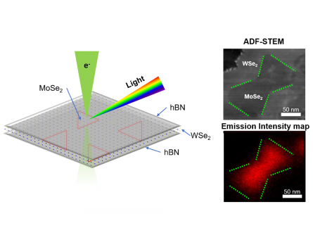
On the left is an illustration of the experimental setup from this study. Molybdenum diselenide nanodots, represented by red triangles, are embedded in tungsten diselenide and encapsulated by hexagonal boron nitride (hBN) on top and bottom. A focused electron beam in green in a scanning transmission electron microscope (STEM) is aimed at the structure. The emitted light is collected to generate an intensity map. On the upper right is a dark-field STEM image of the molybdenum diselenide nanodot embedded inside tungsten diselenide. Dotted green lines mark the contour of the nanodot. On the lower right is an artificially colored light emission intensity map of the same region, with the localized emission from the nanodot visible.
In a study published in ACS Photonics, the scientists demonstrated how these nanodots — tiny islands of a few nanometers — emit different colors based on their size. “If you have the opportunity to have localized light emission from these materials that are relevant in quantum technologies and electronics, it’s very exciting,” said Nasim Alem, Penn State associate professor of materials science and engineering and co-corresponding author on the study. “Envision getting light from a zero-dimensional point in your field, like a dot in space, and not only that, but you can also control it. You can control the frequency. You can also control the wavelength where it comes from.”
To achieve this, the team embedded nanodots of molybdenum diselenide into tungsten diselenide then used a beam of electrons — a technique known as cathodoluminescence — to make the structure emit light. “By combining a light detection tool with a transmission electron microscope, which is a powerful microscope that uses electrons to image samples, you can see much finer details than with other techniques,” said Saiphaneendra Bachu, the study’s first author and a recent Penn State doctoral graduate. “Electrons have tiny wavelengths, so the resolution is incredibly high, letting you detect light from one tiny dot separately from another nearby dot.”
The researchers observed that larger dots glowed differently than smaller ones. Dots less than 10 nanometers wide emitted light at higher frequencies, a result Alem attributed to quantum confinement, where energy levels become discrete inside extremely tight spaces. This allowed the group to confirm that nanodots confined excitons—particle pairs capable of transporting energy without carrying a net charge — at the molybdenum diselenide and tungsten diselenide interface.
Such precise control over light emission could benefit future quantum computing systems —where excitons can facilitate faster, more secure processing — and everyday technologies like high-resolution displays. “Think about how OLED displays work,” Bachu said. “Each pixel has its own tiny light source behind it, so you can control the exact color or brightness of each one. This lets the screen show true black and accurate colors like red, green, and blue. If you improve this process, you make the picture much sharper and more vibrant.”
According to the team, the key is adjusting the material’s band gap, the energy threshold that electrons must cross to emit light. While each member of the 2D materials family—such as molybdenum disulfide, tungsten disulfide, molybdenum diselenide, and tungsten diselenide—has its own band gap, mixing them allows scientists to fine-tune the emitted light more precisely.
“This is just the tip of the iceberg,” Alem said. “By exploring the role of atomic structure, chemistry, and other factors in controlling light emission while expanding on lessons learned in this study, we can move this research to the next level and develop practical applications.”
Researchers from the University of North Texas, the University of Pennsylvania, and Japan’s National Institute for Materials Science are co-authors. The study was partly funded and supported by the Fulbright Scholar program, the National Science Foundation, and the European Union’s Horizon 2020 Research and Innovation Programs.