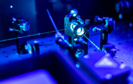
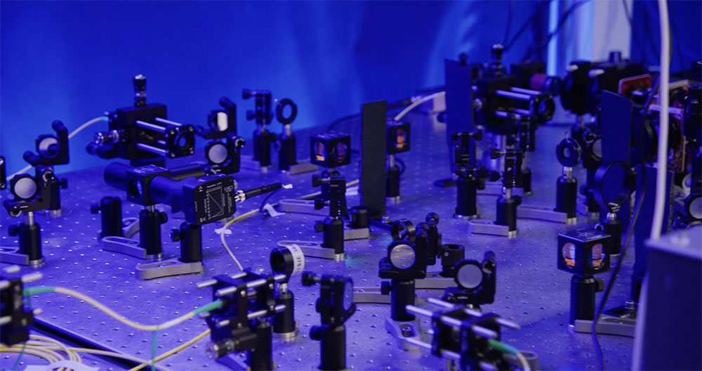
An NTT Research scientist, dressed in a cleanroom suit, working in NTT Research’s laser lab.
NTT Research is playing the long game, tackling challenges that others shy away from. While many R&D labs focus on a relatively near-term ROI for research, NTT is more patient, taking a page from storied labs like Bell Labs and Xerox PARC that prioritize bigger, riskier but potentially more transformative bets. Its website declares: “Our goal is to upgrade reality.”
The looming energy crisis in AI
And they believe they’ve found a way to give a reality an upgrade in photonics. Kazuhiro Gomi, president and CEO of NTT Research, compares their work in optical integrated circuits to the invention of the transistor, with the potential to support the industrialization of AI by dramatically reducing its energy consumption and boosting its computational power. “One of the scary sides of AI now is energy consumption,” Gomi said. “It’s going through the roof.”
As a case in point, consider that data centers now consume 1-2% of overall global power, according to Goldman Sachs, which projects that amount to reach 3–4% by 2030. AI is one of the bigger drivers of the growth. For instance, a typical ChatGPT query can take about ten times more energy than a normal Google search. Wells Fargo projects that AI power demand will surge 550% from 2024 to 2026, from 8 TWh in 2024 to 52.

Kazu Gomi
This urgency stems from the fundamental limitations of current electronic technology. As Gomi explains, “Part of the problem is that Moore’s Law has kind of saturated,” he said. The principle, which Gordon E. Moore devised in 1965, predicted that the number of transistors on a microchip would double about every roughly two years. But it’s getting tougher to cram more transistors onto silicon wafers. “Demand is growing for computation, but the only thing you can do to fulfill the demand is basically stack up the servers, which creates more heat and energy requirements.”
The ‘transistor moment’ for photonics
This is where NTT Research believes photonics can make a difference. By using light instead of electricity to transmit data, optical integrated circuits promise to dramatically increase bandwidth and speed while curbing energy consumption. “Optics is much more energy efficient when it comes to higher bandwidth,” Gomi explained. “At lower bandwidth, the difference between optics and electronics is not significant, but as clock speed gets higher, optics becomes much more energy efficient.”
Photonics, the science and technology of light, is emerging as a powerful tool to accelerate core mathematical operations in AI. Deep learning, an AI staple, heavily relies on matrix multiplication — a computationally intensive task. Yet photonic systems offer a elegant alternative for these calculations. “Basically, with analog processing, you can do the multiplications via optics,” Gomi said.
The fundamental principle behind photonic matrix multiplication is simple in principle. “When you align two light beams, the output of those two beams is actually the multiplication of the two incoming lights,” Gomi said. “This happens naturally, meaning it’s super low energy.”
Addressing the data bottleneck
While the energy efficiency of optics and electronics is comparable at lower bandwidths, optics becomes significantly more energy-efficient as clock speeds increase. This advantage becomes especially pronounced in high-performance computing scenarios, such as those deep learning models with billions or even trillions of parameters. As AI models continue to grow in size and complexity, memory bandwidth and data transfer become growing bottlenecks.
Here, Gomi emphasized another benefit of photonics, pointing to the potential of light to enable “high-speed memory processing and data transmission.” The advantages of photonics are twofold. First, the energy efficiency of optical data transmission surpasses that of electronics, especially at higher bandwidths required for the constant data exchange between memory and GPUs in AI training. This exchange is particularly intensive in deep learning, which involves multiple stages: the forward pass, where input data flows through the network. Next, the model calculates the loss, comparing the model’s output to the expected result. After that, the error is propagated back through the network in the back propagation step and finally, the model updates is parameters, adjusted weights and biases before continuing to see if the model converges.
This iterative process of forward and backward passes, coupled with constant parameter updates, makes deep learning exceptionally computationally intensive. Each pass requires millions or even billions of mathematical operations, all of which consume energy and generate heat.
Using photons rather than electronics for the data transfer between memory and processing units could enable more efficient, and ultimately more sustainable deep learning.
The promise of thin-film lithium niobate in next-gen circuits
Central to NTT Research’s vision is lithium niobate, a material with a long history in optical communications that researchers have reimagined in thin-film form. This breakthrough lays the groundwork for a novel era of photonic integrated circuits, where active devices like laser oscillators, amplifiers, and modulators can be integrated onto a single chip. “Recently, we found a way to make lithium niobate into a thin film and put it on a silicon wafer, which creates a lot of interesting applications,” Gomi said.
Known as thin film lithium niobate (TFLN), the material has strong electro-optic effects and nonlinear optical characteristics, making it well suited for manipulating light on chip-scale devices. TFLN also allows for the creation of densely packed photonic circuits with higher performance, bandwidth, and functionality compared to silicon-based chips. In addition, the material enables the development of various optical components, including modulators, switches, filters, and frequency converters. “We’re focusing on multiplications, laser oscillators, amplifiers, and modulators — active devices on the chip, rather than just point A to point B data transmission,” Gomi said.
Advancing laser technology
NTT Research’s innovations extend beyond the realm of TFLN. The company has made significant strides in laser technology, particularly in the development of frequency combs. As Gomi explains, “You can take one incoming laser beam and divide that single wavelength into multiple wavelengths… because it’s coming from a single laser source and being divided into multiple wavelengths, everything is phase-locked.”
This breakthrough in frequency comb technology has the potential to drive progress in wavelength division multiplexing, an integral process in optical communications.
Optical components at NTT Research
NTT Innovative Devices, a sister company to NTT Research, is developing photonic-electronic convergence (PEC) devices. These innovative components combine optical and electronic solutions into a single packaged device, representing the next evolution in integrated circuit technology.
PEC devices promise several advantages over traditional electronic circuits, including higher performance, increased functionality, more compact size, reduced power consumption, reduced heat generation and extremely high speeds with low latency over long distances.
The roadmap for PEC devices is ambitious. According to a press release, “In 2025, NTT Innovative Devices plans to manufacture a third-generation device, an optical engine operating at a transmission capacity of 3.2Tbps across a transmission distance of between 10 meters to 2 kilometers. Additional iterations are planned for 2028 (fourth generation) and 2032 (fifth generation) with transmission speeds of 5Tbps (integrated in the device width of 5mm) and 15Tbps (width of 2mm), respectively, and transmission distances of 1 centimeter to 1 kilometer and approximately 1 centimeter, respectively.”
While the full realization of these technologies may be years away, the potential impact on the AI landscape could be significant. “It’s not going to happen overnight, but it should make AI more sustainable,” Gomi said.