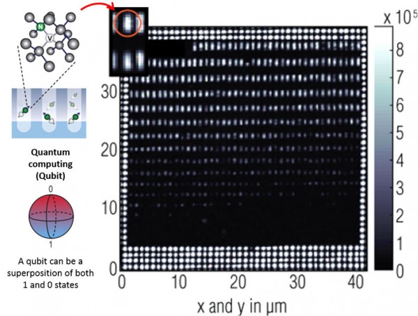
(Bottom left) Classical computers store data in bits that can have a state of either 0 or 1. Quantum computers store data in quantum bits (qubits) that can have a superposition of both 0 and 1 states. (Top left) A graphical representation of nitrogen vacancy (NV) qubits fabricated within diamond. (Right) These NVs were made in precise, dense arrays (μm = micrometers) for future quantum computers.
The Science
For decades scientists have known that a quantum computer—a device that stores and manipulates information in quantum objects such as atoms or photons—could theoretically perform certain calculations far faster than today’s computing schemes. But building the “parts” for a quantum computer is a monumental research task. One promising approach involves using the quantum “spin” property of nitrogen-vacancy (NV) centers in diamonds to store and process data. But properly placing these centers is a major challenge. Recently researchers constructed chains of NV centers in diamond with more precision than any previous effort.
The Impact
Diamond nanophotonics technology is a major contender for future optical computers. This work provides a wholly suitable pathway for the large-scale production of quantum logic gates for quantum computers that that approach the power of the human mind.
Summary
Scientists at the Massachusetts Institute of Technology created a wholly suitable pathway for the large-scale production of quantum logic gates. These gates are a critical component for quantum computing architectures. At the Center for Functional Nanomaterials, the researchers fabricated the silicon-based stencils. They used the stencils to pattern the NV centers. The stencils possessed features as small as 2 nanometers—nearly 10 times smaller than any previous demonstration. These devices are compatible with densities required for quantum computers.
Within diamonds, nitrogen vacancies have electron spin states that could be useful for future quantum computers. The NV electron spin triplet levels can be readily manipulated to create long-lasting states (exceeding milliseconds) at room temperature and even longer states (approaching one second) at the temperature of liquid nitrogen. To extend this approach to create more qubits, researchers devised a fabrication technique that produced well-spaced ensembles of several NVs. The spacing is required to allow the states to couple so they last longer. Their technique is based on masks produced from 270-nanometer-thick, silicon-based stencils, enabling 1-nanometer defects to be packed onto the surface. The team’s approach combined the low full-width half-maximum of the atomic force microscopy tip implantation with the quick patterning available using electron beam lithography. The team used the stencils to reach a regime where the nitrogen distribution is no longer limited by the size of the opening on the stencil but by the basic process of implanted nitrogen scattering in the diamond lattice. The team’s work opens the door to scalable creation of isolated spin ensembles for next-generation quantum computing.


