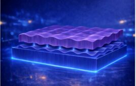
Illustration – Homo- and heterostructures. Image: @tsarcyanide/MIPT Press Office
A physical effect known as superinjection underlies modern light-emitting diodes (LEDs) and lasers. For decades this effect was believed to occur only in semiconductor heterostructures—that is, structures composed of two or more semiconductor materials.
Researchers from the Moscow Institute of Physics and Technology have found superinjection to be possible in homostructures, which are made of a single material. This opens up entirely new prospects for the development of light sources.
The paper came out Feb. 21 in the journal Semiconductor Science and Technology.
Semiconductor light sources, such as lasers and LEDs, are at the core of modern technology. They enable laser printers and high-speed Internet. But a mere 60 years ago, no one would imagine semiconductors being used as materials for bright light sources.
The problem was that to generate light, such devices require electrons and holes—the free charge carriers in any semiconductor—to recombine. The higher the concentration of electrons and holes, the more often they recombine, making the light source brighter.
However, for a long time, no semiconductor device could be manufactured to provide a sufficiently high concentration of both electrons and holes.
The solution was found in the 1960s by Zhores Alferov and Herbert Kroemer. They proposed to use heterostructures, or “sandwich” structures, consisting of two or more complementary semiconductors instead of just one. If one places a semiconductor between two semiconductors with wider bandgaps and applies a forward bias voltage, the concentration of electrons and holes in the middle layer can reach values that are orders of magnitude higher than those in the outer layers.
his effect, known as superinjection, underlies modern semiconductor lasers and LEDs. Its discovery earned Alferov and Kroemer the Nobel Prize in physics in 2000.
However, two arbitrary semiconductors cannot make a viable heterostructure. The semiconductors need to have the same period of the crystal lattice. Otherwise, the number of defects at the interface between the two materials will be too high, and no light will be generated. In a way, this would be similar to trying to screw a nut on a bolt whose thread pitch does not match that of the nut.
Since homostructures are composed of just one material, one part of the device is a natural extension of the other. Although homostructures are easier to fabricate, it was believed that homostructures could not support superinjection and therefore are not a viable basis for practical light sources.
Igor Khramtsov and Dmitry Fedyanin from the Moscow Institute of Physics and Technology made a discovery that drastically changes the perspective on how light-emitting devices can be designed. The physicists found that it is possible to achieve superinjection with just one material. What is more, most of the known semiconductors can be used.
“In the case of silicon and germanium, superinjection requires cryogenic temperatures, and this casts doubt on the utility of the effect. But in diamond or gallium nitride, strong superinjection can occur even at room temperature,” Fedyanin said. This means that the effect can be used to create mass market devices.
According to the new paper, superinjection can produce electron concentrations in a diamond diode that are 10,000 times higher than those previously believed to be ultimately possible. As a result, diamond can serve as the basis for ultraviolet LEDs thousands of times brighter than what the most optimistic theoretical calculations predicted.
“Surprisingly, the effect of superinjection in diamond is 50 to 100 times stronger than that used in most mass market semiconductor LEDs and lasers based on heterostructures,” Khramtsov pointed out.
The physicists emphasized that superinjection should be possible in a wide range of semiconductors, from conventional wide-bandgap semiconductors to novel two-dimensional materials. This opens up new prospects for designing highly efficient blue, violet, ultraviolet, and white LEDs, as well as light sources for optical wireless communication (Li-Fi), new types of lasers, transmitters for the quantum Internet and optical devices for early disease diagnostics.