Computers use switches to perform calculations. A complex film with “quantum wells” — regions that allow electron motion in only two dimensions — can be used to make efficient switches for high-speed computers. For the first time, this oxide film exhibited a phenomenon, called resonant tunneling, in which electrons move between quantum wells at a specific voltage. This behavior allowed an extremely large ratio (about 100,000:1) between two states, which can be used in an electronic device as an ON/OFF switch to perform mathematical calculations.
To meet our exponentially growing need for computing power without a corresponding jump in energy use, scientists need more efficient electronic versions of switches to perform calculations. Efficient switches need materials that switch between well-defined ON/OFF states. The results of this study could lead to a new class of energy-efficient electronics because these materials can ensure the electronic switches are ON or OFF. These electronic switches could lower power consumption in electronics enabling, for example, the development of high-speed supercomputers and cell phones with longer battery life.
In the quantum mechanical phenomenon called resonant tunneling, electrons that are in a well-defined quantum well (or quantum state) can move to an alternate quantum well with an applied voltage. The voltage can be used to switch the electron from an ON to an OFF state. Scientists can use resonant tunneling to develop high-speed switches for electronics. However, the phenomena of resonant tunneling has largely been limited to small numbers of materials because the materials cannot have any defects for tunneling to occur a specific voltage. Researchers led by Oak Ridge National Laboratory grew thin films of nearly defect free, crystalline oxide materials that exhibit resonant tunneling, which means that the materials have the structural and electrical properties needed to develop materials for oxide-based electronics. Scientists made the complex oxide film using a technique called pulsed laser epitaxy. Deposited films had atomically sharp interfaces. At each interface in the complex oxide, there was a two-dimensional electron gas (2DEG). In this region of the material, electrons move freely in two dimensions. These 2DEGs could be considered as quantum wells that spatially confine electrons. The electrons can cross the barrier (that is, tunnel) between the wells through an atomically thin layer. When the electron tunnels through the barrier, the material properties change because the electrons have moved from a highly insulating to a highly conducting state—translating to OFF or ON states, like a switch. The ability to grow high-quality, complex oxide-based quantum wells furthers our understanding of the tunneling phenomena and will enable the development of novel energy-efficient devices based on oxide materials.
Source: U.S. Department of Energy
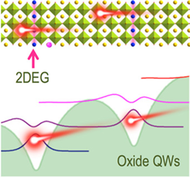
Efficient control of electron motion can be used to reduce the power requirements of computers. “Quantum wells” (QW) are regions that allow electron motion in only two dimensions. The lines (bottom) in the schematic show the probability of finding electrons in the structure. The structure is a complex oxide (top) with columns (stacked blue dots corresponding to an added element) where the electrons are free to move in only two dimensions. This is a special type of quantum well called a two-dimensional electron gas (2DEG). Image: Image courtesy of Ho Nyung Lee, Oak Ridge National Laboratory