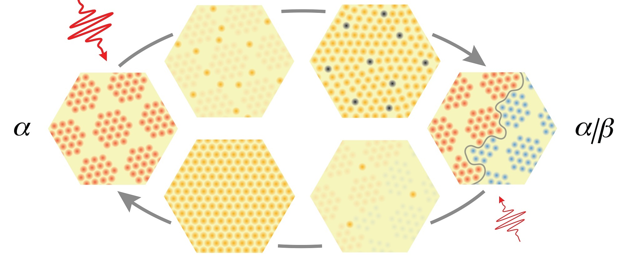
In experiments at SLAC, single pulses of laser light were used to switch tantalum disulfide from one state to another and back again. Clockwise from left: A single light pulse turns the material from its initial, alpha state (red) into a mixture of alpha and beta (blue) states that are separated by domain walls (right). A second light pulse dissolves the domain walls and the material returns to its original state. Switches like this could potentially lead to the development of new types of data storage devices. (DOI: 10.1126/sciadv.aau5501)
Scientists from the Department of Energy’s SLAC National Accelerator Laboratory and the Massachusetts Institute of Technology have demonstrated a surprisingly simple way of flipping a material from one state into another, and then back again, with single flashes of laser light.
This switching behavior is similar to what happens in magnetic data storage materials, and making the switch with laser light could offer a new way to read and write information in next-generation data storage devices, among other unprecedented applications, says Nuh Gedik, the study’s principal investigator at MIT.
The team reported their results in Science Advances.
In today’s devices, information is stored and retrieved by flipping the spin of electrons with a magnetic field.
“But here we flipped a different material property known as charge density waves,” says Alfred Zong, a graduate student in Gedik’s group and one of the study’s lead authors.
Charge density waves are periodic peaks and valleys in the way electrons are distributed in a material. They are motionless, like icy waves on a frozen lake.
Scientists want to learn more about these waves because they often coexist with other interesting material properties, such as the ability to conduct electricity without loss at relatively high temperatures, and could potentially be related to those properties.
The new study focused on tantalum disulfide, a material with charge density waves that are all oriented in the same direction in what’s called the alpha state.
When the researchers zapped a thin crystal of the material with a very brief laser pulse, some of the waves flipped into a beta state with a different electron orientation, and the alpha and beta regions were separated by domain walls.
A second flash of light dissolved the domain walls and returned the material to its pure alpha state.
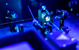
These changes in the material, which had never been seen before, were detected with SLAC’s instrument for ultrafast electron diffraction (UED), a high-speed “electron camera” that probes the motions of a material’s atomic structure with a powerful beam of very energetic electrons.
“We were looking for other effects in our experiment, so we were taken by complete surprise when we saw that we can write and erase domain walls with single light pulses,” says Xijie Wang, head of SLAC’s UED group.
Anshul Kogar, a postdoctoral researcher in Gedik’s group, says, “The domain walls are a particularly interesting feature because they have properties that differ from the rest of the material.”
For example, they might play a role in the drastic change seen in tantalum disulfide’s electrical resistance when it’s exposed to ultrashort light pulses, which was previously observed by another group.
SLAC staff scientist Xiaozhe Shen, one of the study’s lead authors on Wang’s team, says, “UED allowed us to analyze in detail how the domains formed over time, how large they were and how they were distributed in the material.”
The researchers also found that they can fine-tune the process by adjusting the temperature of the crystal and the energy of the light pulse, giving them control over the material switch.
In a next step, the team wants to gain even more control, for example by shaping the light pulse in a way that it allows generating particular domain patterns in the material.
“The fact that we can tune a material in a very simple manner seems very fundamental,” Wang says.
“So fundamental, in fact, that it could turn out to be an important step toward using light in creating the exact material properties we want.”
Additional contributions to this study came from Harvard University. The project was funded by the DOE Office of Science and the Gordon and Betty Moore Foundation.