Research & Development World

  • R&D World Home
  • Topics
    • Aerospace
    • Automotive
    • Biotech
    • Careers
    • Chemistry
    • Environment
    • Energy
    • Life Science
    • Material Science
    • R&D Management
    • Physics
  • Technology
    • 3D Printing
    • A.I./Robotics
    • Software
    • Battery Technology
    • Controlled Environments
      • Cleanrooms
      • Graphene
      • Lasers
      • Regulations/Standards
      • Sensors
    • Imaging
    • Nanotechnology
    • Scientific Computing
      • Big Data
      • HPC/Supercomputing
      • Informatics
      • Security
    • Semiconductors
  • R&D Market Pulse
  • R&D 100
    • Call for Nominations: The 2025 R&D 100 Awards
    • R&D 100 Awards Event
    • R&D 100 Submissions
    • Winner Archive
    • Explore the 2024 R&D 100 award winners and finalists
  • Resources
    • Research Reports
    • Digital Issues
    • R&D Index
    • Subscribe
    • Video
    • Webinars
  • Global Funding Forecast
  • Top Labs
  • Advertise
  • SUBSCRIBE

Smallest-Ever Optical Frequency Comb Developed

By Ecole Polytechnique Federale de Lausanne | February 12, 2019

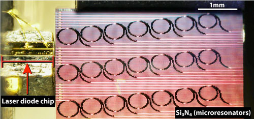
A photograph of the microresonator-frequency comb system. Image: Arslan Raja/EPFL

Optical frequency combs are laser sources whose spectrum consists of a series of discrete, equally spaced frequency lines that can be used for precise measurements. In the last two decades, they have become a major tool for applications such as precise distance measurement, spectroscopy, and telecommunications.

Most of the commercially available optical frequency comb sources based on mode-lock lasers are large and expensive, limiting their potential for use in large volumes and portable applications. Although chip-scale versions of optical frequency combs using microresonators were first demonstrated in 2007, a fully integrated form has been hindered by high material losses and complex excitation mechanisms.

Research teams led by Tobias J. Kippenberg at Ecole Polytechnique Federale de Lausanne (EPFL) and Michael L. Gorodetsky at the Russian Quantum Center have now built an integrated soliton microcomb operating at a repetition rate of 88 GHz using a chip-scale indium phosphide laser diode and the silicon nitride (Si3N4) microresonator. At only 1 cm3 in size, the device is the smallest of its kind to-date (Nature Communications, “Electrically pumped photonic integrated soliton microcomb”).

The silicon nitride microresonator is fabricated using a patented photonic Damascene reflow process that yields unprecedentedly low losses in integrated photonics. These ultra-low loss waveguides bridge the gap between the chip-based laser diode and the power levels required to excite the dissipative Kerr soliton states, which underly the generation of optical frequency combs.

The method uses commercially available chip-based indium phosphide lasers as opposed to conventional bulk laser modules. In the reported work, a small portion of the laser light is reflected back to the laser due to intrinsic scattering from the microresonator. This direct feedback helps to both stabilize the laser and generate the soliton comb. This shows that both resonator and laser can be integrated on a single chip offering a unique improvement over past technology.

“There is a significant interest in optical frequency comb sources that are electrically driven and can be fully photonically integrated to meet the demands of next-generation applications, especially LIDAR and information processing in data-centers,” says Kippenberg. “This not only represents a technological advancement in the field of dissipative Kerr solitons, but also provides an insight into their nonlinear dynamics, along with fast feedback from the cavity.”

The whole system can fit in a volume of less than 1 cm3 and can be controlled electrically.

“The compactness, easy tuning method, low cost and low repetition rate operation make this microcomb system interesting for mass-manufacturable applications,” says PhD student Arslan Sajid, the lead author of the study. “Its main advantage is fast optical feedback, which eliminates the need for active electronic or any other on-chip tuning mechanism.”

The scientists now aim to demonstrate an integrated spectrometer and multi-wavelength source and to improve the fabrication process and the integration method further to push the microcomb source at a microwave repetition rate.

Related Articles Read More >

Illustration of ultracold atoms (gold) flowing frictionlessly along a laser boundary (green), representing the quantum phenomenon of edge states.
MIT physicists directly observe frictionless ‘edge state’ flow in ultracold atoms, offering a glimpse of super-efficient electronics
NTT Research scientist in cleanroom suit working on advanced photonic equipment
NTT Research bets light-based computing can tackles AI’s energy crisis
Scientists claim to generate world’s strongest terahertz radiation
SLAC fires up the world’s most powerful X-ray laser: LCLS-II ushers in a new era of science
rd newsletter
EXPAND YOUR KNOWLEDGE AND STAY CONNECTED
Get the latest info on technologies, trends, and strategies in Research & Development.
RD 25 Power Index

R&D World Digital Issues

Fall 2024 issue

Browse the most current issue of R&D World and back issues in an easy to use high quality format. Clip, share and download with the leading R&D magazine today.

Research & Development World
  • Subscribe to R&D World Magazine
  • Enews Sign Up
  • Contact Us
  • About Us
  • Drug Discovery & Development
  • Pharmaceutical Processing
  • Global Funding Forecast

Copyright © 2025 WTWH Media LLC. All Rights Reserved. The material on this site may not be reproduced, distributed, transmitted, cached or otherwise used, except with the prior written permission of WTWH Media
Privacy Policy | Advertising | About Us

Search R&D World

  • R&D World Home
  • Topics
    • Aerospace
    • Automotive
    • Biotech
    • Careers
    • Chemistry
    • Environment
    • Energy
    • Life Science
    • Material Science
    • R&D Management
    • Physics
  • Technology
    • 3D Printing
    • A.I./Robotics
    • Software
    • Battery Technology
    • Controlled Environments
      • Cleanrooms
      • Graphene
      • Lasers
      • Regulations/Standards
      • Sensors
    • Imaging
    • Nanotechnology
    • Scientific Computing
      • Big Data
      • HPC/Supercomputing
      • Informatics
      • Security
    • Semiconductors
  • R&D Market Pulse
  • R&D 100
    • Call for Nominations: The 2025 R&D 100 Awards
    • R&D 100 Awards Event
    • R&D 100 Submissions
    • Winner Archive
    • Explore the 2024 R&D 100 award winners and finalists
  • Resources
    • Research Reports
    • Digital Issues
    • R&D Index
    • Subscribe
    • Video
    • Webinars
  • Global Funding Forecast
  • Top Labs
  • Advertise
  • SUBSCRIBE