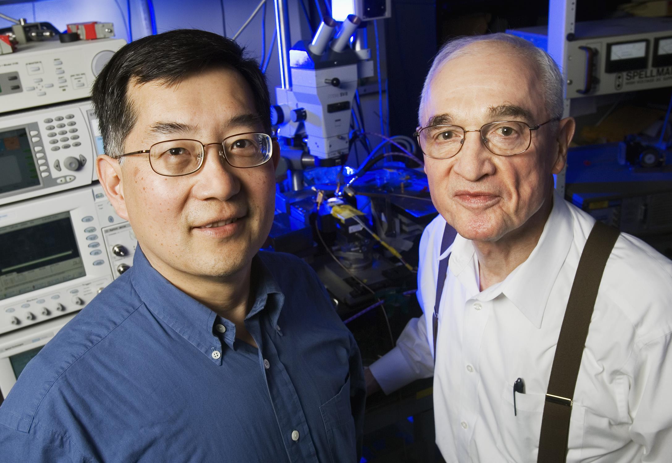
Milton Feng and Nick Holonyak, Jr.
In 2004, electrical engineering pioneers Nick Holonyak, Jr. and Milton Feng at the University of Illinois invented the transistor laser — a three-port device that incorporated quantum-wells in the base and an optical cavity — increasing its capacity to transmit data one hundred-fold. Two recent studies by the researchers are expected to significantly impact the fundamental modulation bandwidth of the transistor and the laser operation for energy-efficient high speed data transfer in optical and 5G wireless communications.
“The transistor (point-contact) invented by John Bardeen and Walter Brattain in 1947 revealed the operating principles of the emitter current injection, the base electron-hole recombination, and the collector current output,” explains Milton Feng, the Holonyak Chair professor emeritus of electrical and computer engineering at Illinois. “The three-terminal transistor replaced the fragile vacuum tube for fast reliable electrical signal switching and amplification, and has made possible a revolution in modern electronics, communications, and computer technologies.”
“We are especially grateful to John Bardeen for bringing transistor research to Urbana in 1951, and changing all of our lives world-wide with the new quantum-physics and solid state devices,” stated Nick Holonyak Jr., Bardeen’s first graduate student, the Bardeen Chair professor emeritus of electrical and computer engineering and physics. In 2004, Feng and Holonyak realized the radiative recombination energy (light) at the base of an III-V heterojunction bipolar transistor could be modulated to be a signal and a three-port device that can harness the intricate physics between electrons and light.
“The fastest way for current to switch in a semiconductor material is for the electrons to jump between bands in the material in a process called tunneling,” Feng says. “Light photons help shuttle the electrons across, a process called intra-cavity photon-assisted tunneling, making the device much faster.”
The laser transistor differs from the Bardeen and Brattain transistor in which the current gain is dependent on the ratio of the base electron-hole (e-h) spontaneous recombination lifetime to the emitter-collector transit time. The Feng and Holonyak transistor laser current gain depends upon the base (e-h) stimulated recombination, the base dielectric relaxation transport, and the collector stimulated tunneling.
In two recent papers, published in the Journal of Applied Physics, Feng — along with Holonyak and graduate researchers Junyi Qiu, and Curtis Wang — have established the principles of operation for tunneling modulation of a quantum well transistor laser with current amplification and optical output via intra-cavity photon-assisted tunneling.
“We consider these two papers related to intra-cavity tunneling modulation of the transistor will change the fundamental speed operation of the transistor and the laser modulation,” Feng says.
In their article, “Tunneling modulation of a quantum well-transistor laser,” (DOI: 10.1063/1.4967922), the authors explain that stimulated e-h recombination operating under the influence of quantum-well assistance in the base, and stimulated optical modulation under the influence of intra-cavity photon-assisted tunneling (ICPAT) at the collector. The authors named their new and novel idea as the “Feng-Holonyak Intra-Cavity Photon-Assisted Tunneling (FH-ICPAT).”
“The tunneling gain mechanism is the result of the unique transistor laser base transport properties under the influence of FH-ICPAT and base dielectric relaxation, which yields fast carrier base transport and fast recombination than the original Bardeen transistor,” explains Wang. “The voltage and current dependence of the tunneling current gain and optical modulation have been revealed in detail. Although the analysis is carried out for the transistor laser intra-cavity photon-assisted tunneling, the operation mechanism should apply in general to tunneling collector transistors of various design configurations.”
In a companion AIP article (“Intra-cavity photon-assisted tunneling collector-base voltage-mediated electron-hole spontaneous-stimulated recombination transistor laser”; DOI: 10.1063/1.4942222), the authors explained how optical absorption and modulation in a p-n junction diode for a direct-gap semiconductor can be enhanced by photon-assisted tunneling in the presence of optical cavity and photon-field in a transistor laser.
“In the transistor laser, the coherent photons generated at the base quantum-well interact with the collector field and ‘assist’ optical cavity electron tunneling from the valence band of the base to the energy state of conduction band of the collector,” Feng says. “The stimulated light output can be modulated by either base current injection via stimulated optical generation or base-collector junction bias via optical absorption.
“In this work, we studied the intra-cavity coherent photon intensity on photon-assisted tunneling in the transistor laser and realize photon field-dependent optical absorption. This FH-ICPAT in a transistor laser is the unique property of voltage (field) modulation and the basis for ultrahigh speed direct laser modulation and switching.
“We remain indebted to John Bardeen, our mentor, for his lifelong continuing interest in the transistor (parallel to the BCS theory), the effect of the electron and the hole (e-h) in helping to originate the diode laser and LED, and in addition now leading to the e-h recombination (electrical and optical) transistor laser,” Feng adds.
This work, carried out at the Micro & Nanotechnology Lab at Illinois, has been supported, in part, by the Air Force Office Scientific Research.