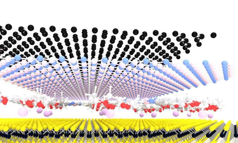
Cross sectional view of the stack of two-dimensional materials. The monolayer electrolyte in the middle allows the ions (pink spheres) to be toggled between two locations. The location of the ions sets the state of the memory. Image: Fullerton Group
For the past 60 years, the electronics industry and the average consumer have benefited from the continuous miniaturization, increased storage capacity and decreased power consumption of electronic devices.
However, this era of scaling that has benefited humanity is rapidly coming to end. To continue shrinking the size and power consumption of electronics, new materials and new engineering approaches are needed.
Susan Fullerton, assistant professor of chemical and petroleum engineering at the University of Pittsburgh’s Swanson School of Engineering, is tackling that challenge by develop next-generation electronics based on all two-dimensional materials.
These “all 2-D” materials are similar to a sheet of paper—if the paper were only a single molecule thick.
Her research into these super-thin materials was recognized by the National Science Foundation with a $540,000 CAREER award, which supports early-career faculty who have the potential to serve as academic role models in research and education and to lead advances in the mission of their department or organization.
“The advent of new computing paradigms is pushing the limit of what traditional semiconductor devices can provide,” Fullerton said. “For example, machine learning will require nanosecond response speeds, sub-volt operation, 1,000 distinct resistance states, and other aspects that no existing device technology can provide.
“We’ve known for a long time that ions—like the ones in lithium-ion batteries—are very good at controlling how charge moves in these ultra-thin semiconductors,” she noted. “In this project, we are reimagining the role of ions in high-performance electronics. By layering successive molecule-sized layers on top of each other, we aim to increase storage capacity, decrease power consumption, and vastly accelerate processing speed .”
To build this all 2-D device, Fullerton and her group invented a new type of ion-containing material, or electrolyte, which is only a single molecule thick. This “monolayer electrolyte” will ultimately introduce new functions that can be used by the electronic materials community to explore the fundamental properties of new semiconductor materials and to develop electronics with completely new device characteristics.
According to Fullerton, there are several important application spaces where the materials and approaches developed in this CAREER research could have an impact: information storage, brain-inspired computing, and security, in particular.
In addition to developing the monolayer electrolytes, the NSF award will support a Ph.D. student and postdoctoral researcher, as well as an outreach program to inspire curiosity and engagement of K-12 and underrepresented students in materials for next-generation electronics.
Specifically, Dr. Fullerton has developed an activity where students can watch the polymer electrolytes used in this study crystallize in real-time using an inexpensive camera attached to a smart phone or iPad.
The CAREER award will allow Fullerton to provide this microscope to classrooms so that the teachers can continue exploring with their students.
“When the students get that portable microscope in their hands—they get really creative,” she said. “After they watch what happens to the polymer, they go exploring. They look at the skin on their arm, the chewing gum out of their mouth, or the details of the fabric on their clothing. It’s amazing to watch this relatively inexpensive tool spark curiosity in the materials that are all around them, and that’s the main goal.”
Fullerton noted that her research takes a truly novel approach to ion utilization, which has traditionally been avoided by the semiconductor community.
“Ions are often ignored because if you cannot control their location, they can ruin a device. So the idea of using ions not just as a tool to explore fundamental properties, but as an integral device component is extremely exciting and risky,” explained Fullerton.
“If adopted, ions coupled with 2-D materials could represent a paradigm shift in high-performance computing because we need brand new materials with exciting new physics and properties that are no longer limited by size.”


