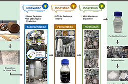
14-nm polystyrene lines on 28-nm pitch after PMMA removal fabricated by DSA using 193-nm immersion based 84-nm pitch pre-pattern (left) and demonstration of the ability to repair a 200-nm gap in the pre-pattern (right). Image: imec |
At
this week’s SPIE Advanced Lithography conference in San Jose, Calif.,
imec plans to announce the successful implementation of the world’s
first 300-mm fab-compatible directed self-assembly (DSA) process line
all under one roof in imec’s 300-mm cleanroom fab. The upgrade of an
academic lab-scale DSA process flow to a fab-compatible flow was
realized in collaboration with the University of Wisconsin, AZ
Electronic Materials and Tokyo Electron Ltd. Imec’s DSA collaboration
aims to address the critical hurdles to take DSA from the academic
lab-scale environment into high-volume manufacturing.
Directed
Self-Assembly (DSA) is gaining momentum as a means for extending
optical lithography beyond its current limits. DSA is an alternative
patterning technology that enables frequency multiplication through the
use of block copolymers. When used in conjunction with an appropriate
pre-pattern that directs the orientation for patterning, DSA can reduce
the pitch of the final printed structure. Moreover, DSA can be used to
repair defects and repair uniformity in the original print. This repair
feature is especially useful in combination with EUV lithography, which
today is characterized by local variation in the CD (critical
dimension), especially in case of small contacts.
Imec
now has the complete toolset on-site including a dedicated and
specially configured DSA coater/developer manufactured by TEL with
installed DSA materials in gallon-size quantities, the metrology toolkit
including DSA defect inspection, and in-house pattern transfer
capabilities all in a representative 300mm cleanroom fab environment.
With established 248nm, 193nm (dry and immersion) and EUV lithography
tool sets on site, imec is uniquely positioned to study DSA defectivity
aiming at increasing the pattern reliability of DSA for semiconductor
fab standards. Moreover, imec aims at further developing the
possibilities of DSA repair in combination with EUV lithography, pushing
imec’s ambition to bring EUV Lithography to production level.
Kurt
Ronse, Director Lithography Department at imec: “We are excited with
this achievement, as this enables us to expand the scope of our research
offering and toolset bringing more value to our partners. The
availability of a DSA processing line enables us to further push the
limits of 193nm immersion lithography and overcome some of the critical
concerns for EUV lithography. This allows us to further push the limits
of Moore’s law.”
“With
this process, imec has taken an important step towards fulfilling the
low cost, high resolution promise of bottom up DSA lithography,” says
Ralph Dammel, CTO of AZ Electronic Materials. “We are committed to
providing the high performance materials the industry needs to make DSA a
commercial reality.”
Prof.
Paul Nealey: “Juan de Pablo and I and the University of Wisconsin team
are very pleased to have the opportunity to partner with imec. Our work
together results in unprecedented integration of DSA with
manufacturing-ready tools and materials, allows investigation of the
ultimate potential and possible limits of DSA not possible in an
academic setting, and provides exceptional educational opportunities for
our students. We are gratified to be on a pathway with imec towards
commercialization of technology we have spent almost 15 years
developing.”
This
research offering is part of imec’s Advanced lithography program,
available to imec’s partners in its core CMOS programs. Imec’s key core
CMOS partners are Globalfoundries, INTEL, Micron, Panasonic, Samsung,
TSMC, Elpida, Hynix, Fujitsu and Sony.


