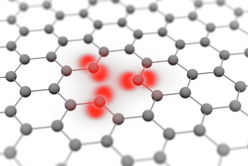
Atomic orbitals of carbon atoms in graphene. (Credit: Vienna University of Technology)
An electron microscope can’t just snap a photo like a mobile phone camera can. The ability of an electron microscope to image a structure – and how successful this imaging will be – depends on how well you understand the structure. Complex physics calculations are often needed to make full use of the potential of electron microscopy. An international research team led by TU Wien’s Prof. Peter Schattschneider set out to analyse the opportunities offered by EFTEM, that is energy-filtered transmission electron microscopy. The team demonstrated numerically that under certain conditions, it is possible to obtain clear images of the orbital of each individual electron within an atom. Electron microscopy can therefore be used to penetrate down to the subatomic level – experiments in this area are already planned. The study has now been published in the physics journal Physical Review Letters.
In search of the electron orbital
We often think of atomic electrons as little spheres that circle around the nucleus of the atom like tiny planets around a sun. This image is barely reflected in reality, however. The laws of quantum physics state that the position of an electron cannot be clearly defined at any given point in time. The electron is effectively smeared across an area close to the nucleus. The area that could contain the electron is called the orbital. Although it has been possible to calculate the shape of these orbitals for a long time, efforts to image them with electron microscopes have been unsuccessful to date.
“We have calculated how we might have a chance of visualising orbitals with an electron microscope”, says Stefan Löffler from the University Service Centre for Transmission Electron Microscopy (USTEM) at TU Wien. “Graphene, which is made of just one single layer of carbon atoms, is an excellent candidate for this task. The electron ray is able to pass easily through the graphene with hardly any elastic scattering. An image of the graphene structure can be created with these electrons.”
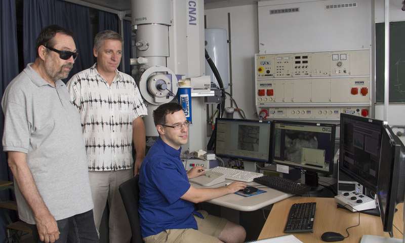
Peter Schattschneider, Johannes Bernardi, Stefan Löffler. (Credit: Vienna University of Technology)
Researchers have been aware of the principle of “energy-filtered transmission electron microscopy” (EFTEM) for some time. EFTEM can be used to create quite specific visualisations of certain kinds of atoms whilst blocking out the others. For this reason, it is often used today to analyse the chemical composition of microscopic samples. “The electrons shot through the sample can excite the sample’s atoms”, explains Stefan Löffler. “This costs energy, so when the electrons emerging emerge from the sample, they are slower than when they entered it. This velocity and energy change is characteristic for certain excitations of electron orbitals within the sample.”
After the electrons have passed through the sample, a magnetic field sorts the electrons by energy. “A filter is used to block out electrons that aren’t of interest: the recorded image contains only those electrons that carry the desired information.”
Defects can be helpful
The team used simulations to investigate how this technique could help reach a turning point in the study of electron orbitals. While doing so, they discovered something that actually facilitated the imaging of individual orbitals: “The symmetry of the graphene has to be broken”, says Stefan. “If, for instance, there is a hole in the graphene structure, the atoms right beside this hole have a slightly different electronic structure, making it possible to image the orbitals of these atoms. The same thing can happen if a nitrogen atom rather than a carbon atom is found somewhere in the graphene. When doing this, it’s important to focus on the electrons found within a narrow and precise energy window, minimise certain aberrations of the electromagnetic lens and, last but not least, use a first-rate electron microscope.” All of these issues can be overcome, however, as the research group’s calculations show.
The Humboldt-Universität zu Berlin, the Universität Ulm, and McMaster University in Canada also worked alongside the TU Wien on the study in a joint FWF-DFG project (“Towards orbital mapping”, I543-N20) and a FWF Erwin-Schrödinger project (“EELS at interfaces”, J3732-N27). Ulm is currently developing a new, high-performance transmission electron microscope that will be used to put these ideas into practice in the near future. Initial results have already exceeded expectations.