Research & Development World

  • R&D World Home
  • Topics
    • Aerospace
    • Automotive
    • Biotech
    • Careers
    • Chemistry
    • Environment
    • Energy
    • Life Science
    • Material Science
    • R&D Management
    • Physics
  • Technology
    • 3D Printing
    • A.I./Robotics
    • Software
    • Battery Technology
    • Controlled Environments
      • Cleanrooms
      • Graphene
      • Lasers
      • Regulations/Standards
      • Sensors
    • Imaging
    • Nanotechnology
    • Scientific Computing
      • Big Data
      • HPC/Supercomputing
      • Informatics
      • Security
    • Semiconductors
  • R&D Market Pulse
  • R&D 100
    • Call for Nominations: The 2025 R&D 100 Awards
    • R&D 100 Awards Event
    • R&D 100 Submissions
    • Winner Archive
    • Explore the 2024 R&D 100 award winners and finalists
  • Resources
    • Research Reports
    • Digital Issues
    • R&D Index
    • Subscribe
    • Video
    • Webinars
  • Global Funding Forecast
  • Top Labs
  • Advertise
  • SUBSCRIBE

A Little Impurity Makes Nanolasers Shine

By Australian National University | July 5, 2016

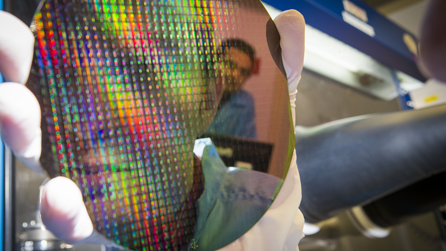
Tim Burgess holds a silicon wafer on which nanostructures are grown. (Credit: Stuart Hay, ANU)

Scientists at ANU (The Australian National University) have improved the performance of tiny lasers by adding impurities, in a discovery which will be central to the development of low-cost biomedical sensors, quantum computing, and a faster internet.

Researcher Tim Burgess added atoms of zinc to lasers one hundredth the diameter of a human hair and made of gallium arsenide – a material used extensively in smartphones and other electronic devices.

The impurities led to a 100 times improvement in the amount of light from the lasers.

“Normally you wouldn’t even bother looking for light from nanocrystals of gallium arsenide – we were initially adding zinc simply to improve the electrical conductivity,” said Burgess, a Ph.D. student in the ANU Research School of Physics and Engineering.

“It was only when I happened to check for light emission that I realised we were onto something.”

Gallium arsenide is a common material used in smartphones, photovoltaic cells, lasers and light-emitting diodes (LEDs), but is challenging to work with at the nanoscale as the material requires a surface coating before it will produce light.

Previous ANU studies have shown how to fabricate suitable coatings.

The new result complements these successes by increasing the amount of light generated inside the nanostructure, said research group leader Professor Chennupati Jagadish, from the ANU Research School of Physics Sciences.

“It is an exciting discovery and opens up opportunities to study other nanostructures with enhanced light emission efficiency so that we can shrink the size of the lasers further,” he said.

Burgess said that the addition of the impurity to gallium arsenide, a process called doping, improved not only the light emission.

“The doped gallium arsenide has a very short carrier lifetime of only a few picoseconds, which meant it would be well suited to use in high speed electronics components,” he said. “The doping has really has given these nanolasers a performance edge.”

The research is published in Nature Communications.


Related Articles Read More >

Floating solar mats clean polluted water — and generate power
Nanodots enable fine-tuned light emission for sharper displays and faster quantum devices
New photon-avalanching nanoparticles could enable next-generation optical computers
New “nose-computer interface” aims to upgrade Rover’s nose for better drug detection methods
rd newsletter
EXPAND YOUR KNOWLEDGE AND STAY CONNECTED
Get the latest info on technologies, trends, and strategies in Research & Development.
RD 25 Power Index

R&D World Digital Issues

Fall 2024 issue

Browse the most current issue of R&D World and back issues in an easy to use high quality format. Clip, share and download with the leading R&D magazine today.

Research & Development World
  • Subscribe to R&D World Magazine
  • Enews Sign Up
  • Contact Us
  • About Us
  • Drug Discovery & Development
  • Pharmaceutical Processing
  • Global Funding Forecast

Copyright © 2025 WTWH Media LLC. All Rights Reserved. The material on this site may not be reproduced, distributed, transmitted, cached or otherwise used, except with the prior written permission of WTWH Media
Privacy Policy | Advertising | About Us

Search R&D World

  • R&D World Home
  • Topics
    • Aerospace
    • Automotive
    • Biotech
    • Careers
    • Chemistry
    • Environment
    • Energy
    • Life Science
    • Material Science
    • R&D Management
    • Physics
  • Technology
    • 3D Printing
    • A.I./Robotics
    • Software
    • Battery Technology
    • Controlled Environments
      • Cleanrooms
      • Graphene
      • Lasers
      • Regulations/Standards
      • Sensors
    • Imaging
    • Nanotechnology
    • Scientific Computing
      • Big Data
      • HPC/Supercomputing
      • Informatics
      • Security
    • Semiconductors
  • R&D Market Pulse
  • R&D 100
    • Call for Nominations: The 2025 R&D 100 Awards
    • R&D 100 Awards Event
    • R&D 100 Submissions
    • Winner Archive
    • Explore the 2024 R&D 100 award winners and finalists
  • Resources
    • Research Reports
    • Digital Issues
    • R&D Index
    • Subscribe
    • Video
    • Webinars
  • Global Funding Forecast
  • Top Labs
  • Advertise
  • SUBSCRIBE