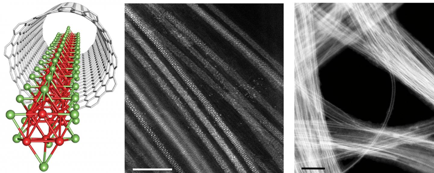
This is a schematic and electron microscopy images of single wires of molybdenum telluride formed inside carbon nanotubes. These 1D reaction vessels are a good fit for the wires, and confine the chemical reactions which create them to one direction. Epitaxial (layer by layer) growth can then proceed along the inner walls of the tubes. Image: Tokyo Metropolitan University
Researchers from Tokyo Metropolitan University have used carbon nanotube templates to produce nanowires of transition metal monochalcogenide (TMM), which are only three atoms wide in diameter. These are 50 times longer than previous attempts and can be studied in isolation, preserving the properties of atomically quasi “1D” objects.
The team saw that single wires twist when perturbed, suggesting that isolated nanowires have unique mechanical properties which might be applied to switching in nanoelectronics.
Two-dimensional materials have gone from theoretical curiosity to real-life application in the span of less than two decades; the most well known example of these, graphene, consists of well-ordered sheets of carbon atoms. Though we are far from leveraging the full potential of graphene, its remarkable electrical and thermal conductivity, optical properties and mechanical resilience have already led to a wide range of industrial applications. Examples include energy storage solutions, biosensing and even substrates for artificial tissue.
Yet, despite the successful transition from 3D to 2D, the barrier separating 2D and 1D has been significantly more challenging to overcome. A class of materials known as transition metal monochalcogenides (TMMs, transition metal + group 16 element) have received particular interest as a potential nanowire in precision nanoelectronics.
Theoretical studies have existed for over 30 years, and preliminary experimental studies have also succeeded in making small quantities of nanowire, but these were usually bundled, too short, mixed with bulk material or simply low yield, particularly when precision techniques were involved e.g. lithography.
The bundling was particularly problematic; forces known as van der Waals forces would force the wires to aggregate, effectively masking all the unique properties of 1D wires that one might want to access and apply.
Now, a team led by Assistant Professor Yusuke Nakanishi from Tokyo Metropolitan University has succeeded in producing bulk quantities of well-isolated single nanowires of TMM. They used tiny, open-ended rolls of single-layered carbon, or carbon nanotubes (CNTs), to template the assembly and reaction of molybdenum and tellurium into wires from a vapor.
They succeeded in producing single isolated wires of TMM, which were only three atoms thick and 50 times longer than those made using existing methods. These nanometer-sized CNT “test tubes” were also shown to be not chemically bound to the wires, effectively preserving the properties expected from isolated TMM wires. Importantly, they effectively “protected” the wires from each other, allowing for unprecedented access to how these 1D objects behave in isolation.
While imaging these objects using transmission electron microscopy (TEM), the team found that these wires exhibited a unique twisting effect when exposed to an electron beam. Such behavior has never been seen before and is expected to be unique to isolated wires. The transition from a straight to twisted structure may offer a novel switching mechanism when the material is incorporated into microscopic circuits.
The team hopes the ability to make well-isolated 1D nanowires might significantly expand our understanding of the properties and mechanisms behind the function of 1D materials.