Research & Development World

  • R&D World Home
  • Topics
    • Aerospace
    • Automotive
    • Biotech
    • Careers
    • Chemistry
    • Environment
    • Energy
    • Life Science
    • Material Science
    • R&D Management
    • Physics
  • Technology
    • 3D Printing
    • A.I./Robotics
    • Software
    • Battery Technology
    • Controlled Environments
      • Cleanrooms
      • Graphene
      • Lasers
      • Regulations/Standards
      • Sensors
    • Imaging
    • Nanotechnology
    • Scientific Computing
      • Big Data
      • HPC/Supercomputing
      • Informatics
      • Security
    • Semiconductors
  • R&D Market Pulse
  • R&D 100
    • Call for Nominations: The 2025 R&D 100 Awards
    • R&D 100 Awards Event
    • R&D 100 Submissions
    • Winner Archive
    • Explore the 2024 R&D 100 award winners and finalists
  • Resources
    • Research Reports
    • Digital Issues
    • R&D Index
    • Subscribe
    • Video
    • Webinars
  • Global Funding Forecast
  • Top Labs
  • Advertise
  • SUBSCRIBE

Bending the Norm on Nanowires for Durability

By KAUST | May 24, 2019

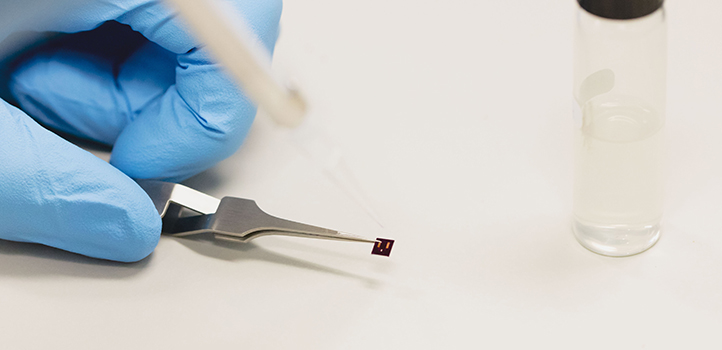
The team suspended silver nanowires from platinum electrodes over their custom-made TEM chips. Image: KAUST

New methods of arranging silver nanowires make them more durable, shows a study by KAUST. These nanowires form flexible, transparent conductive layers that can be used for improved solar cells, strain sensors and next-generation mobile phones.

Applying nanotechnology in electronic devices requires rigorous testing of individual tiny components to ensure they will stand up to use. Silver nanowires show great promise as connectors that could be arranged in flexible, near-transparent meshes for touchscreens or solar cells, but it is unclear how they will respond to prolonged stresses from bending and carrying current.

Testing the bulk properties of a large sample of nanoparticles is easy, but not completely revelatory. However, adopting transmission electron microscopy (TEM) makes it possible to examine individual nanoparticles. Ph.D. student Nitin Batra and his supervisor Pedro Da Costa are at the forefront of developing new TEM techniques. This has allowed them to study single silver nanowires in detail.

“A major part of our work has been designing and fabricating sample platform prototypes (or chips) for TEM, which allow us to characterize and manipulate nanomaterials with an unsurpassed spatial resolution,” says Batra.

To improve on expensive commercially available chips that contain a very fragile membrane to support nanoparticles, Batra and Da Costa, with help from Ahad Syed of the Nanofabrication Core Lab at KAUST, have now submitted to patent their own robust, reusable chips that don’t require a membrane.

The researchers suspended silver nanowires from platinum electrodes over their custom-made TEM chips and applied a range of voltages until the nanowires failed due to heating by the electrical current. They found that straight nanowires tended to snap when they reached a certain high current density, at points determined by local structural defects.

More interesting behavior was seen when the nanowires were bent from the beginning. These samples tended to buckle instead of snapping at high voltage and exhibited an ability to self-heal because they remained held together by the carbon coating on the outside of the wires. Some nanowires even exhibited resonant vibrations, like the harmonics on a guitar string, before they failed.

“Many devices are expected to undergo repeated bending and twisting by the end-user, which means that it is not realistic to limit the study of the electrical response of silver nanowires to straight configurations,” says Batra. “Our results suggest that the failure rate of such devices could be minimized by using bent nanowires instead of straight ones. The self-healing capability could effectively delay the breakdown of the circuit.”

Related Articles Read More >

Floating solar mats clean polluted water — and generate power
Nanodots enable fine-tuned light emission for sharper displays and faster quantum devices
New photon-avalanching nanoparticles could enable next-generation optical computers
New “nose-computer interface” aims to upgrade Rover’s nose for better drug detection methods
rd newsletter
EXPAND YOUR KNOWLEDGE AND STAY CONNECTED
Get the latest info on technologies, trends, and strategies in Research & Development.
RD 25 Power Index

R&D World Digital Issues

Fall 2024 issue

Browse the most current issue of R&D World and back issues in an easy to use high quality format. Clip, share and download with the leading R&D magazine today.

Research & Development World
  • Subscribe to R&D World Magazine
  • Enews Sign Up
  • Contact Us
  • About Us
  • Drug Discovery & Development
  • Pharmaceutical Processing
  • Global Funding Forecast

Copyright © 2025 WTWH Media LLC. All Rights Reserved. The material on this site may not be reproduced, distributed, transmitted, cached or otherwise used, except with the prior written permission of WTWH Media
Privacy Policy | Advertising | About Us

Search R&D World

  • R&D World Home
  • Topics
    • Aerospace
    • Automotive
    • Biotech
    • Careers
    • Chemistry
    • Environment
    • Energy
    • Life Science
    • Material Science
    • R&D Management
    • Physics
  • Technology
    • 3D Printing
    • A.I./Robotics
    • Software
    • Battery Technology
    • Controlled Environments
      • Cleanrooms
      • Graphene
      • Lasers
      • Regulations/Standards
      • Sensors
    • Imaging
    • Nanotechnology
    • Scientific Computing
      • Big Data
      • HPC/Supercomputing
      • Informatics
      • Security
    • Semiconductors
  • R&D Market Pulse
  • R&D 100
    • Call for Nominations: The 2025 R&D 100 Awards
    • R&D 100 Awards Event
    • R&D 100 Submissions
    • Winner Archive
    • Explore the 2024 R&D 100 award winners and finalists
  • Resources
    • Research Reports
    • Digital Issues
    • R&D Index
    • Subscribe
    • Video
    • Webinars
  • Global Funding Forecast
  • Top Labs
  • Advertise
  • SUBSCRIBE