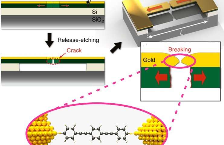
Research & Development World

  • R&D World Home
  • Topics
    • Aerospace
    • Automotive
    • Biotech
    • Careers
    • Chemistry
    • Environment
    • Energy
    • Life Science
    • Material Science
    • R&D Management
    • Physics
  • Technology
    • 3D Printing
    • A.I./Robotics
    • Software
    • Battery Technology
    • Controlled Environments
      • Cleanrooms
      • Graphene
      • Lasers
      • Regulations/Standards
      • Sensors
    • Imaging
    • Nanotechnology
    • Scientific Computing
      • Big Data
      • HPC/Supercomputing
      • Informatics
      • Security
    • Semiconductors
  • R&D Market Pulse
  • R&D 100
    • Call for Nominations: The 2025 R&D 100 Awards
    • R&D 100 Awards Event
    • R&D 100 Submissions
    • Winner Archive
    • Explore the 2024 R&D 100 award winners and finalists
  • Resources
    • Research Reports
    • Digital Issues
    • R&D Index
    • Subscribe
    • Video
    • Webinars
  • Global Funding Forecast
  • Top Labs
  • Advertise
  • SUBSCRIBE

Cracking the Problem of Mass Produced Molecular Junctions

By Delft University of Technology | August 31, 2018

Credit: TU Delft

Nanogap electrodes, basically pairs of electrodes with a nanometer-sized gap between them, are attracting attention as scaffolds to study, sense, or harness molecules, the smallest stable structures found in nature. So far, this has been realised using the common methods of mechanically controlled break junctions, scanning tunneling microscopy-based break junctions,or electromigrated break junctions. These techniques, however, are not useful for applications due to their lack of scalability. A team from TU Delft in collaboration with researchers from the KTH Royal Institute of Technology in Sweden has now developed a novel way of fabricating molecular junctions.

The researchers started by depositing a thin film of brittle titanium nitride (TiN) on a silicon wafer (see figure). Thereafter, small gold wires could be deposited on top of the brittle TiN. The researchers observed that the TiN film is under high residual tensile strain due to the fabrication process. Consequently, when detaching the titanium nitride layer from its underlying substrate via a process called release etching, tiny cracks form to release the strain – similar to cracks that sometimes form in the glazing of pottery.

This cracking process is the key to the new junction fabrication method. Gold wires running across the cracks are stretched and eventually break. The gaps in the gold wires that thus appear are as small as a single molecule. In addition, the dimensions of these junctions can be controlled by controlling the strain in TiN using conventional microfabrication technology. Furthermore, the researchers managed to link single molecules to the gapped gold wires to measure their electrical conductance.

This novel technology could be used to produce molecular junctions in a scalable fashion – allowing millions of them to be manufactured in parallel. The methodology can also be extended to other classes of materials by substituting gold with any electrode material that exhibits interesting electrical, chemical, and plasmonic properties for applications in molecular electronics and spintronics, nanoplasmonics, and biosensing.


Related Articles Read More >

Floating solar mats clean polluted water — and generate power
Nanodots enable fine-tuned light emission for sharper displays and faster quantum devices
New photon-avalanching nanoparticles could enable next-generation optical computers
New “nose-computer interface” aims to upgrade Rover’s nose for better drug detection methods
rd newsletter
EXPAND YOUR KNOWLEDGE AND STAY CONNECTED
Get the latest info on technologies, trends, and strategies in Research & Development.
RD 25 Power Index

R&D World Digital Issues

Fall 2024 issue

Browse the most current issue of R&D World and back issues in an easy to use high quality format. Clip, share and download with the leading R&D magazine today.

Research & Development World
  • Subscribe to R&D World Magazine
  • Enews Sign Up
  • Contact Us
  • About Us
  • Drug Discovery & Development
  • Pharmaceutical Processing
  • Global Funding Forecast

Copyright © 2025 WTWH Media LLC. All Rights Reserved. The material on this site may not be reproduced, distributed, transmitted, cached or otherwise used, except with the prior written permission of WTWH Media
Privacy Policy | Advertising | About Us

Search R&D World

  • R&D World Home
  • Topics
    • Aerospace
    • Automotive
    • Biotech
    • Careers
    • Chemistry
    • Environment
    • Energy
    • Life Science
    • Material Science
    • R&D Management
    • Physics
  • Technology
    • 3D Printing
    • A.I./Robotics
    • Software
    • Battery Technology
    • Controlled Environments
      • Cleanrooms
      • Graphene
      • Lasers
      • Regulations/Standards
      • Sensors
    • Imaging
    • Nanotechnology
    • Scientific Computing
      • Big Data
      • HPC/Supercomputing
      • Informatics
      • Security
    • Semiconductors
  • R&D Market Pulse
  • R&D 100
    • Call for Nominations: The 2025 R&D 100 Awards
    • R&D 100 Awards Event
    • R&D 100 Submissions
    • Winner Archive
    • Explore the 2024 R&D 100 award winners and finalists
  • Resources
    • Research Reports
    • Digital Issues
    • R&D Index
    • Subscribe
    • Video
    • Webinars
  • Global Funding Forecast
  • Top Labs
  • Advertise
  • SUBSCRIBE