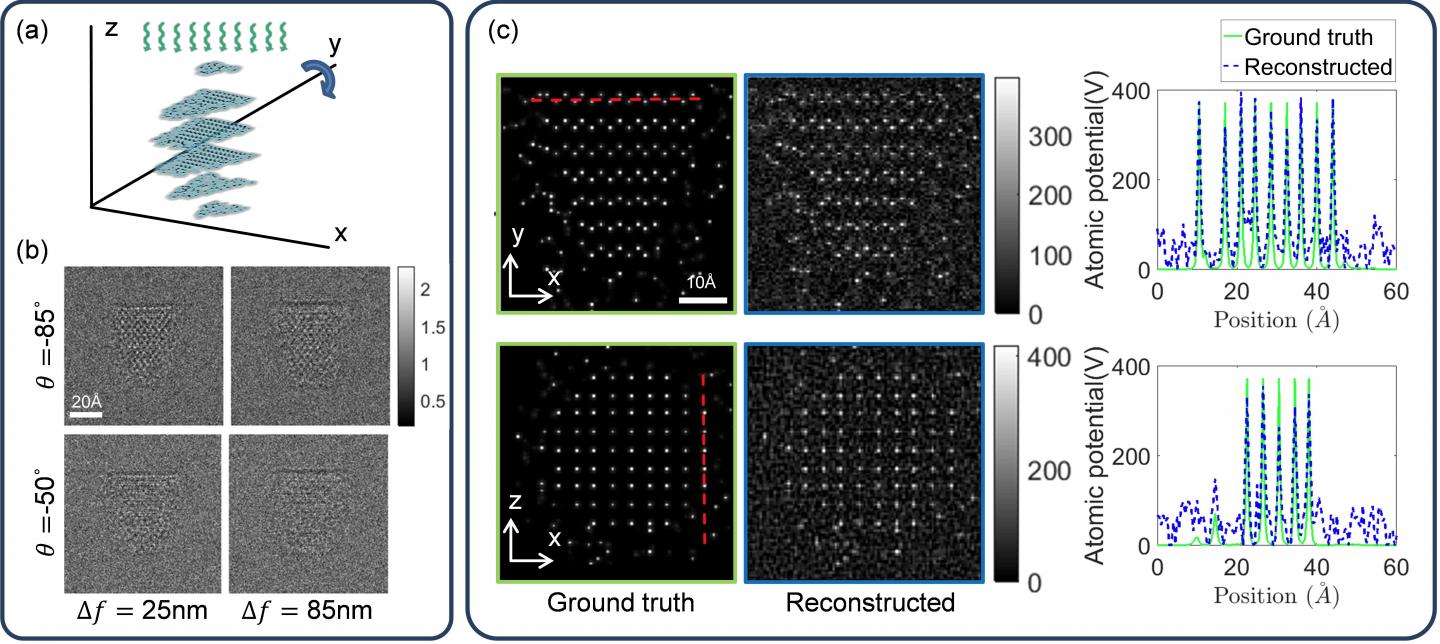
This is a schematic of proposed TEM 3-D atomic imaging with multi-slice method with four examples of noisy intensity measurements at different angles of rotation, and 3-D atomic potential reconstructions and 1-D cross-sections along x and y directions. Credit: David Ren
Understanding the microscopic structure of a material is key to understanding how it functions and its functional properties. Advances in fields like materials science have increasingly pushed abilities to determine these features to even higher resolutions. One technique for imaging at nanoscale resolution, transmission electron microscopy (TEM), is one example of promising technology in this area. Scientists recently found a way to harness the power of TEM to measure the structure of a material at the highest possible resolution – determining the 3D position of every individual atom.
Presenting their work at the OSA Imaging and Applied Optics Congress 25-28 June, in Orlando, Florida, USA, a team of researchers has demonstrated a technique using TEM tomography to determine the 3D positions of strongly scattering atoms. Through simulation, the group showed that it is possible to reconstruct the atomic potentials with atomic resolution using only image intensity measurements, and that it’s possible to do so on molecules that are very sensitive to electron beams.
“Transmission electron microscopy is used extensively in both materials science and biology,” said Colin Ophus, National Center for Electron Microscopy, Lawrence Berkeley National Lab, Berkeley, California, and a member of the research team. “Because we fully solve the nonlinear propagation of the electron beam, our tomographic reconstruction method will enable more quantitative reconstruction of weakly scattering samples, at higher or even atomic resolution.”
Similar to the way computerized tomography (CT) scans performed for medical imaging in hospitals are built using a series of two-dimensional cross-sectional images at different increments, electron tomography constructs a three-dimensional volume by rotating samples incrementally, collecting two-dimensional images. While most CT imaging in hospitals is done with x-rays to determine features of larger things like bones, the beams of electrons used in TEM allows researchers to look with significantly higher resolution, down to the atomic scale.
“However, on the atomic scale we cannot neglect the very complex quantum mechanical effects of the sample on the electron beam,” Ophus said. “This means in our work, we must use a much more sophisticated algorithm to recover the atomic structure than those used in an MRI or CT scan.”
The TEM setup the group used measured the energy intensity that hits the microscope’s sensor, which is proportional to the number of electrons that hit the sensor, a number that depends on how the electron beam is configured for each experiment. Using the intensity data, the new algorithm designed by the group stitched the two-dimensional projected images into a 3D volume.
Making the jump to three dimensions with large fields of view, however, can tax computers exponentially more than dealing with single 2D images. To work around this, they modified their algorithm to be used on graphic processing units (GPUs), which can perform many times more mathematical operations in parallel than typical computer processing units (CPUs).
“We are able to obtain results in a reasonable amount of time for realistic sample dimensions,” said David Ren, a member of the team.
With generally weaker bonds between their atoms, biomolecules can be notoriously difficult to study using TEM because the electron beams used to study a metal alloy, for example, would typically tear a biomolecule apart. Lowering the electron dosage in a sample, though, can create images that are so noisy, other algorithms currently in use can’t reconstruct a 3D image. Thanks to a more precise physical model, the team’s new algorithm has the ability.
Now that they have fully developed the reconstruction algorithm, the team said they hope to apply what they’ve observed from simulations to experimental data. They plan to make all of their reconstruction codes available as open source for the wider research community.