|

Long-wavelength terahertz light is invisible—it’s at the farthest end of the
far infrared—but it’s useful for everything from detecting explosives at the
airport, to designing drugs, to diagnosing skin cancer. Now, for the first time,
scientists at the U.S. Department of Energy’s Lawrence Berkeley National
Laboratory (Berkeley Lab) and the University
of California at Berkeley have demonstrated a microscale
device made of grapheme, whose strong response to light at terahertz
frequencies can be tuned with exquisite precision.
“The heart of our device is an array made of graphene ribbons only
millionths of a meter wide,” says Feng Wang of Berkeley Lab’s Materials
Sciences Division, who is also an assistant professor of physics at UC
Berkeley, and who led the research team. “By varying the width of the ribbons
and the concentration of charge carriers in them, we can control the collective
oscillations of electrons in the microribbons.”
The name for such collective oscillations of electrons is plasmons.
“Plasmons in high-frequency visible light happen in 3D metal nanostructures,”
Wang says. The colors of medieval stained glass, for example, result from
oscillating collections of electrons on the surfaces of nanoparticles of gold,
copper, and other metals, and depend on their size and shape. “But graphene is
only one atom thick, and its electrons move in only two dimensions. In 2D
systems, plasmons occur at much lower frequencies.”
The wavelength of terahertz radiation is measured in hundreds of micrometers,
yet the width of the graphene ribbons in the experimental device is only one to
four micrometers each.
“A material that consists of structures with dimensions much smaller than
the relevant wavelength, and which exhibits optical properties distinctly
different from the bulk material, is called a metamaterial,” says Wang. “So we
have not only made the first studies of light and plasmon coupling in graphene,
we’ve also created a prototype for future graphene-based metamaterials in the
terahertz range.”
The team reports their research in Nature Nanotechnology.
|

How to push the
plasmons
In 2D graphene, electrons have a tiny rest mass and respond quickly to
electric fields. A plasmon describes the collective oscillation of many
electrons, and its frequency depends on how rapidly waves in this electron sea
slosh back and forth between the edges of a graphene microribbon. When light of
the same frequency is applied, the result is “resonant excitation,” a marked
increase in the strength of the oscillation—and simultaneous strong absorption
of the light at that frequency. Since the frequency of the oscillations is
determined by the width of the ribbons, varying their width can tune the system
to absorb different frequencies of light.
The strength of the light-plasmon coupling can also be
affected by the concentration of charge carriers—electrons and their positively
charged counterparts, holes. One remarkable characteristic of graphene is that
the concentration of its charge carriers can easily be increased or decreased
simply by applying a strong electric field—so-called electrostatic doping.
The Berkeley
device incorporates both these methods for tuning the response to terahertz
light. Microribbon arrays were made by depositing an atom-thick layer of carbon
on a sheet of copper, then transferring the graphene layer to a silicon-oxide
substrate and etching ribbon patterns into it. An ion gel with contact points
for varying the voltage was placed on top of the graphene.
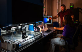
The gated graphene microarray was illuminated with terahertz
radiation at beamline 1.4 of Berkeley Lab’s Advanced Light Source, and
transmission measurements were made with the beamline’s infrared spectrometer.
In this way the research team demonstrated coupling between light and plasmons
that was stronger by an order of magnitude than in other 2D systems.
A final method of controlling plasmon strength and terahertz
absorption depends on polarization. Light shining in the same direction as the
graphene ribbons shows no variations in absorption according to frequency. But
light at right angles to the ribbons—the same orientation as the oscillating
electron sea—yields sharp absorption peaks. What’s more, light absorption in
conventional 2D semiconductor systems, such as quantum wells, can only be
measured at temperatures near absolute zero. The Berkeley team measured prominent absorption
peaks at room temperature.
“Terahertz radiation covers a spectral range that’s
difficult to work with, because until now there have been no tools,” says Wang. “Now we have the beginnings of a toolset for working in this range, potentially
leading to a variety of graphene-based terahertz metamaterials.”
The Berkeley
experimental setup is only a precursor of devices to come, which will be able
to control the polarization and modify the intensity of terahertz light and
enable other optical and electronic components, in applications from medical
imaging to astronomy—all in two dimensions.