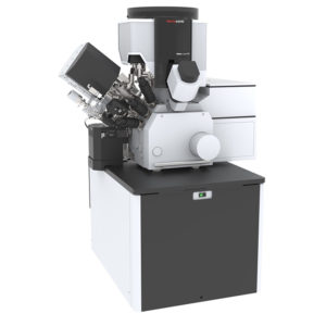
Thermo Scientific Helios 5 Laser PFIB
Thermo Scientific Helios 5 Laser PFIB system, released by Thermo Fisher Scientific, is an advanced focused ion-beam-scanning electron microscope (FIB-SEM) with a fully integrated femtosecond laser that quickly characterizes millimeter-scale volumes of material in 3D with nanometer resolution.
The Helios 5 Laser PFIB combines the best-in-class Thermo Scientific Elstar SEM Column for ultra-high-resolution imaging and advanced analytical capabilities with a plasma FIB column for top performance at all operating conditions, and a femtosecond laser that enables in-situ ablation at material removal rates not previously obtained by a commercially available product. The Helios 5 Laser PFIB is part of the fifth generation of the Helios family.
“The Helios 5 Laser PFIB dramatically accelerates the pace of research for both academic and industrial users, allowing them to characterize materials in a matter of minutes versus the days it took before,” said Rosy Lee, vice president of materials science at Thermo Fisher. “Not only can researchers quickly and accurately image statistically relevant, site-specific, millimeter-size cross-sections at nanoscale resolution, they can also set up large-volume 3D analyses to be automatically completed overnight, freeing up the microscope for other uses.”
The Helios 5 Laser PFIB allows researchers to obtain accurate large-volume 3D and sub-surface data up to 15,000 times faster than a typical Gallium ion source focused ion beam (Ga-FIB). For many materials, a large cross-section of hundreds of microns can be milled by the Helios 5 Laser PFIB in less than five minutes. Serial-section tomography is now possible with this combination of Laser and Plasma FIB, and when combined with EDS and EBSD detectors, can be extended to 3D elemental and grain orientation analysis at the millimeter scale.
After close collaboration over several years with McLean Echlin and Tresa Pollock at UC Santa Barbara, the first commercially available units were shipped to The National Institute for Materials Science (NIMS) in Japan and The University of Manchester in Manchester, England, where both organizations are already seeing benefits.
“The system not only performs high-resolution SEM for microstructural analysis but also enables large-volume 3D imaging previously not possible. This should help to greatly advance our understanding of inhomogeneity and deformation mechanisms in materials,” said Dr. Toru Hara, Station Director, Structural Materials Analysis Station, National Institute for Materials Science (NIMS), Japan.
“At Royce, we’re aiming to establish a characterization capability needed to drive forward the microstructural informatics revolution needed for the design of new materials and better understanding of existing ones,” said Regius Prof. Phil Withers, Chief Scientist at the Henry Royce Institute for advanced materials research and innovation. “The Helios 5 Laser PFIB is capable of excising millimeter-sized regions of interest and collecting the massive 3D microstructural datasets at SEM resolutions this requires.”
“I am particularly excited about how this solution extends our ability to conduct correlative workflows and allows us to connect together different analysis techniques. We will be able to reach deeply buried features and interfaces, as well as machine and extract multiple minute test specimens from targeted locations in times not previously achieved by our research team,” according to Dr. Tim Burnett, The University of Manchester.
The Helios 5 Laser PFIB makes it easy for academic and industrial labs to process challenging non-conductive, air-sensitive and beam-sensitive materials. They can also expedite failure analysis while obtaining fast access to buried sub-surface layers often inaccessible with traditional FIB. The FIB-SEM can be used to analyze a variety of materials including metals, batteries, glass, ceramics, paint coatings, polymers, biomaterials and graphite.
Built on the Thermo Scientific Helios 5 platform, the Helios 5 Laser PFIB redefines the standard in high-resolution imaging with high materials contrast; fast, easy and precise high-quality sample preparation for scanning transmission electron microscopy (S/TEM) and Atom Probe Tomography (APT).
For more information, visit: HeliosLaserPFIB.


Tell Us What You Think!