By Clara Ko, Sales and Marketing Manager, Linkam Scientific Instruments
Photovoltaics, ferroelectrics, and piezoelectrics have a suite of remarkable properties, with a long history of electrical applications in everything from ultrasound transducers to solar cells. But there is constant pressure to improve performance, and in this article, we look at how precisely controlling the temperature at which electrical measurements are made is helping researchers to improve their understanding of these materials.
With the demand for microelectronics constantly growing, electronics design and development engineers are being asked to develop materials with ever better characteristics. These include improved signal strength, reduced energy consumption, or better environmental credentials – all while reducing the size and weight of components. Solutions to many of these challenges can be found by fine-tuning the chemical composition and microstructure of the materials used in photovoltaics, ferroelectrics, and piezoelectrics.
But doing this requires a deep understanding of their properties and particularly how their electrical properties vary with temperature. In this article, we highlight two application examples where being able to precisely control the temperature of a material during a measurement has made a significant contribution to understanding its properties.
Application 1: Understanding the kinetic properties of novel organic photovoltaics
Organic photovoltaics (OPVs) – which use carbon-based molecules – have for many years been seen as appealing alternatives to the silicon-based technology that is used in most photovoltaic installations, thanks to their combination of low weight, ability to be formed into thin flexible films, and tailorable properties such as bandgap, transparency, and color. OPVs should also be cheaper to manufacture in high volumes and have the potential to offer a lower environmental impact than silicon photovoltaics.
However, with maximum efficiencies at around 11% (compared to around 30% for the best inorganic photovoltaics) and with limited data available on longevity, OPVs have long suffered from a perception that they’re not efficient enough or stable enough to work in the real world. Fortunately, new materials are changing that, and researchers at Swansea University, U.K., have been developing new tools to better understand their properties under different temperature conditions.
The work has been led by Dr. Wei Li and Professor Ardalan Armin in the Department of Physics, who developed a new approach for measuring quantum efficiency at different temperatures. Their setup, which incorporated a temperature-controlled stage (Figure 1), allowed them to investigate the kinetics of bimolecular recombination of electron-hole pairs for an OPV system (see W. Li, et al., Organic solar cells with near-unity charge generation yield, Energy & Environmental Science, 2021, 14: 6484-6493). Although relatively well-established as a concept, such kinetic studies have up to now proven extremely challenging in practice, especially under real-world conditions.
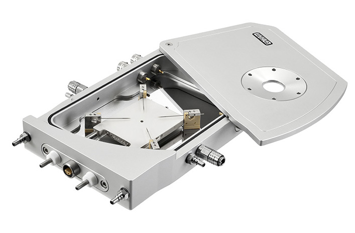
Figure 1: The LTS420E-PB4 temperature-controlled stage used in the work at Swansea University. Along with the precision of temperature control needed for the work (this model has a stability of <0.1 °C), the compactness of such stages facilitates easy integration into analytical setups. The image shows the needle probes that allow the measurement of electrical properties.
The understanding they gained from using this temperature-controlled system enabled them to develop a polymer-non-fullerene OPV blend with the best thick-junction performance achieved to date for any binary organic solar cell – 16.2% power conversion efficiency with a 300 nm junction. This is important because the combination of high efficiency and a thick junction is essential to be able to make OPV-based devices at a large scale using high-throughput deposition techniques such as ‘roll-to-roll’ methods (which struggle to achieve uniform films that are thinner than 100 nm). The team hopes that their research will help pave the way for easily engineered OPVs with improved properties than has hitherto been possible, while overcoming the disadvantages of silicon-based systems.
Application 2: Making low-noise measurements of ferroelectrics and piezoelectrics
Due to their unique properties, ferroelectric and piezoelectric materials play a key role in many research and commercial applications. Ferroelectrics exhibit spontaneous electrical polarization even when the external electric field is zero, with this polarization being switchable by a sufficiently strong electric field applied in the opposite direction – meaning that the material retains a ‘memory’ of the earlier electric field. Piezoelectrics generate an internal electrical field when subjected to mechanical stress, and conversely are deformed when an electric field is applied – making them particularly valuable in equipment for generating and detecting sound waves.
The applications of ferroelectric and piezoelectric materials are numerous, and today they can be found in a wide range of electronic devices, including audio equipment, cell phones, medical diagnostic instruments, cameras, and sensors, among others. Demand for these materials is also growing and with it the need to understand their properties under various conditions, especially temperature.
However, this presents a problem, because measuring the tiny electrical responses from ferroelectrics and piezoelectrics requires that electrical noise is minimized – something that not all temperature-control systems are able to accommodate. The problem is particularly acute when studying thin films, where even small levels of noise can lead to inaccurate results.
Fortunately, a solution is to hand in the form of noise-minimized temperature-control stages (Figure 2). Earthing both the sample pedestal and the chamber enclosure makes the temperature-controlled enclosure an efficient Faraday cage, shielding the sample from ambient electrical noise. This, coupled with a passive ceramic insulator to hold the sample, results in accurate measurements of electrical responses down to very low levels.
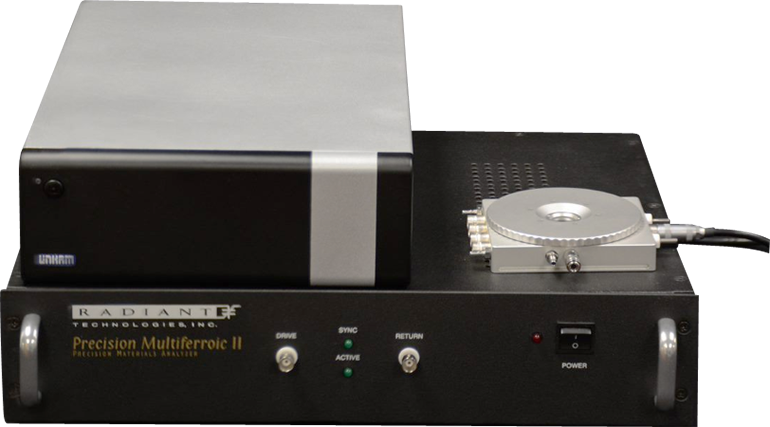
Figure 2: An example of a ferroelectric/piezoelectric tester interfaced with an HFS600E-PB4 temperature-controlled stage (right), offering 0.1° C precision as well as temperature change rates of up to 2.5° C/s. In this case, the system can operate at temperatures of -195° C (or below) up to 600° C, within a gas-tight environment.
Coupling the electrical testing equipment with a dedicated temperature-controlled stage such as this allows electrical measurements of thin ferroelectric and piezoelectric capacitors to be made over a wide temperature range. In addition, the system can also accommodate bulk ceramics or single crystals at up to 300 V – enough to generate full hysteresis loops on the latest lead magnesium niobate-lead titanate (PMN-PT) single-crystal actuators, and to test single-layer or multi-layer materials.
As the option to incorporate temperature control into testing of ferroelectrics and piezoelectrics becomes better known, researchers are increasingly appreciating the value of assessing the effect of temperature on other electrical properties – such as leakage and breakdown voltage. The availability of such an integrated measurement system is therefore helping researchers get a more complete picture of how these materials behave, enabling them to develop more efficient ferroelectric and piezoelectric materials, and expand their application range.
Temperature-controlled stages: Providing a more detailed picture
In conclusion, these examples demonstrate that being able to make electrical measurements of photovoltaics, ferroelectrics, and piezoelectrics under precise temperature control makes it much easier for researchers to obtain fine-grained information on their properties. Such stages, as well as providing the connections or probes needed to make electrical measurements, offer options for investigating the effect of gas purging, controlled vacuum, or humidity.
Moreover, these temperature-controlled stages can also be integrated with other analytical equipment, including X-ray scattering to understand crystal structures and surface composition, Raman spectroscopy and Fourier transform infrared for information on chemical identity, and light microscopy to understand surface morphology.
With these tools available, electronics design and development engineers will be in a better position than ever before to improve photovoltaics, ferroelectrics, and piezoelectrics, and so take advantage of these useful electronic materials.