Research & Development World

  • R&D World Home
  • Topics
    • Aerospace
    • Automotive
    • Biotech
    • Careers
    • Chemistry
    • Environment
    • Energy
    • Life Science
    • Material Science
    • R&D Management
    • Physics
  • Technology
    • 3D Printing
    • A.I./Robotics
    • Software
    • Battery Technology
    • Controlled Environments
      • Cleanrooms
      • Graphene
      • Lasers
      • Regulations/Standards
      • Sensors
    • Imaging
    • Nanotechnology
    • Scientific Computing
      • Big Data
      • HPC/Supercomputing
      • Informatics
      • Security
    • Semiconductors
  • R&D Market Pulse
  • R&D 100
    • Call for Nominations: The 2025 R&D 100 Awards
    • R&D 100 Awards Event
    • R&D 100 Submissions
    • Winner Archive
    • Explore the 2024 R&D 100 award winners and finalists
  • Resources
    • Research Reports
    • Digital Issues
    • R&D Index
    • Subscribe
    • Video
    • Webinars
  • Global Funding Forecast
  • Top Labs
  • Advertise
  • SUBSCRIBE

Innovative Technique Could Pave Way for New Generation of Flexible Electronic Components

By University of Exeter | January 24, 2019

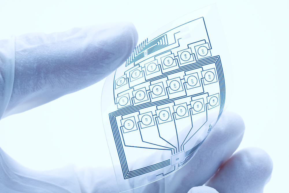
Researchers at the University of Exeter have developed an innovative technique that could help create the next generation of everyday flexible electronics.

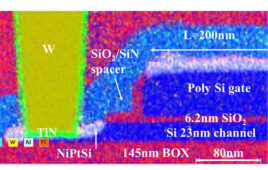
A team of engineering experts have pioneered a new way to ease production of van der Waals heterostructures with high-K dielectrics- assemblies of atomically thin two-dimensional (2-D) crystalline materials.

One such 2-D material is graphene, which comprises of a honeycomb-shaped structure of carbon atoms just one atom thick.

While the advantages of van der Waals heterostructures is well documented, their development has been restricted by the complicated production methods.

Now, the research team has developed a new technique that allows these structures to achieve suitable voltage scaling, improved performance and the potential for new, added functionalities by embedding a high-K oxide dielectric.

The research could pave the way for a new generation of flexible fundamental electronic components.

The research is published in the journal Science Advances.

Dr Freddie Withers, co-author of the paper and from the University of Exeter said: “Our method to embed a laser writable high-K dielectric into various van der Waals heterostructure devices without damaging the neighbouring 2D monolayer materials opens doors for future practical flexible van der Waals devices such as, field effect transistors, memories, photodetectors and LED’s which operate in the 1-2 Volt range”

The quest to develop microelectronic devices to increasingly smaller size underpins the progress of the global semiconductor industry – a collection of companies that includes the tech and communication giants Samsung and Toshiba – has been stymied by quantum mechanical effects.

This means that as the thickness of conventional insulators is reduced, the ease at which electrons can escape through the films.

In order to continue scaling devices ever smaller, researchers are looking at replacing conventional insulators with high-dielectric-constant (high-k) oxides. However, commonly used high-k oxide deposition methods are not directly compatible with 2D materials.

The latest research outlines a new method to embed a multi-functional, nanoscaled high-K oxide, only a within van der Waals devices without degrading the properties of the neighbouring 2D materials.

This new technique allows for the creation of a host of fundamental nano-electronic and opto-electronic devices including dual gated graphene transistors, and vertical light emitting and detecting tunnelling transistors.

Dr Withers added: “The fact we start with a layered 2D semiconductor and convert it chemically to its oxide using laser irradiation allows for high quality interfaces which improve device performance.

“What’s especially interesting for me is we found this oxidation process of the parent HfS2 to take place under laser irradiation even when its sandwiched between 2 neighbouring 2D materials. This indicates that water needs to travel between the interfaces for the reaction to occur.”

Related Articles Read More >

Floating solar mats clean polluted water — and generate power
Nanodots enable fine-tuned light emission for sharper displays and faster quantum devices
New photon-avalanching nanoparticles could enable next-generation optical computers
New “nose-computer interface” aims to upgrade Rover’s nose for better drug detection methods
rd newsletter
EXPAND YOUR KNOWLEDGE AND STAY CONNECTED
Get the latest info on technologies, trends, and strategies in Research & Development.
RD 25 Power Index

R&D World Digital Issues

Fall 2024 issue

Browse the most current issue of R&D World and back issues in an easy to use high quality format. Clip, share and download with the leading R&D magazine today.

Research & Development World
  • Subscribe to R&D World Magazine
  • Enews Sign Up
  • Contact Us
  • About Us
  • Drug Discovery & Development
  • Pharmaceutical Processing
  • Global Funding Forecast

Copyright © 2025 WTWH Media LLC. All Rights Reserved. The material on this site may not be reproduced, distributed, transmitted, cached or otherwise used, except with the prior written permission of WTWH Media
Privacy Policy | Advertising | About Us

Search R&D World

  • R&D World Home
  • Topics
    • Aerospace
    • Automotive
    • Biotech
    • Careers
    • Chemistry
    • Environment
    • Energy
    • Life Science
    • Material Science
    • R&D Management
    • Physics
  • Technology
    • 3D Printing
    • A.I./Robotics
    • Software
    • Battery Technology
    • Controlled Environments
      • Cleanrooms
      • Graphene
      • Lasers
      • Regulations/Standards
      • Sensors
    • Imaging
    • Nanotechnology
    • Scientific Computing
      • Big Data
      • HPC/Supercomputing
      • Informatics
      • Security
    • Semiconductors
  • R&D Market Pulse
  • R&D 100
    • Call for Nominations: The 2025 R&D 100 Awards
    • R&D 100 Awards Event
    • R&D 100 Submissions
    • Winner Archive
    • Explore the 2024 R&D 100 award winners and finalists
  • Resources
    • Research Reports
    • Digital Issues
    • R&D Index
    • Subscribe
    • Video
    • Webinars
  • Global Funding Forecast
  • Top Labs
  • Advertise
  • SUBSCRIBE