In what could be a major step forward for a new generation of solar cells called “concentrator photovoltaics,” University of Michigan researchers have developed a new semiconductor alloy that can capture the near-infrared light located on the leading edge of the visible light spectrum.
Easier to manufacture and at least 25 percent less costly than previous formulations, it’s believed to be the world’s most cost-effective material that can capture near-infrared light — and is compatible with the gallium arsenide semiconductors often used in concentrator photovoltaics.
Concentrator photovoltaics gather and focus sunlight onto small, high-efficiency solar cells made of gallium arsenide or germanium semiconductors. They’re on track to achieve efficiency rates of over 50 percent, while conventional flat-panel silicon solar cells top out in the mid-20s.
“Flat-panel silicon is basically maxed out in terms of efficiency,” said Rachel Goldman, U-M professor of materials science and engineering, and physics, whose lab developed the alloy. “The cost of silicon isn’t going down and efficiency isn’t going up. Concentrator photovoltaics could power the next generation.”
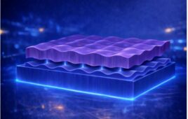
Varieties of concentrator photovoltaics exist today. They are made of three different semiconductor alloys layered together. Sprayed onto a semiconductor wafer in a process called molecular-beam epitaxy–a bit like spray painting with individual elements — each layer is only a few microns thick. The layers capture different parts of the solar spectrum; light that gets through one layer is captured by the next.
But near-infrared light slips through these cells unharnessed. For years, researchers have been working toward an elusive “fourth layer” alloy that could be sandwiched into cells to capture this light. It’s a tall order; the alloy must be cost-effective, stable, durable and sensitive to infrared light, with an atomic structure that matches the other three layers in the solar cell.
Getting all those variables right isn’t easy, and until now, researchers have been stuck with prohibitively expensive formulas that use five elements or more.
To find a simpler mix, Goldman’s team devised a novel approach for keeping tabs on the many variables in the process. They combined on-the-ground measurement methods including X-ray diffraction done at U-M and ion beam analysis done at Los Alamos National Laboratory with custom-built computer modeling.
Using this method, they discovered that a slightly different type of arsenic molecule would pair more effectively with the bismuth. They were able to tweak the amount of nitrogen and bismuth in the mix, enabling them to eliminate an additional manufacturing step that previous formulas required. And they found precisely the right temperature that would enable the elements to mix smoothly and stick to the substrate securely.
“‘Magic’ is not a word we use often as materials scientists,” Goldman said. “But that’s what it felt like when we finally got it right.”
The advance comes on the heels of another innovation from Goldman’s lab that simplifies the “doping” process used to tweak the electrical properties of the chemical layers in gallium arsenide semiconductors. During doping, manufacturers apply a mix of chemicals called “designer impurities” to change how semiconductors conduct electricity and give them positive and negative polarity similar to the electrodes of a battery. The doping agents usually used for gallium arsenide semiconductors are silicon on the negative side and beryllium on the positive side.
The beryllium is a problem–it’s toxic and it costs about 10 times more than silicon dopants. Beryllium is also sensitive to heat, which limits flexibility during the manufacturing process. But the U-M team discovered that by reducing the amount of arsenic below levels that were previously considered acceptable, they can “flip” the polarity of silicon dopants, enabling them to use the cheaper, safer element for both the positive and negative sides.
“Being able to change the polarity of the carrier is kind of like atomic ‘ambidexterity,'” said Richard Field, a former U-M doctoral student who worked on the project. “Just like people with naturally born ambidexterity, it’s fairly uncommon to find atomic impurities with this ability.”
Together, the improved doping process and the new alloy could make the semiconductors used in concentrator photovoltaics as much as 30 percent cheaper to produce, a big step toward making the high-efficiency cells practical for large-scale electricity generation.
“Essentially, this enables us to make these semiconductors with fewer atomic spray cans, and each can is significantly less expensive,” Goldman said. “In the manufacturing world, that kind of simplification is very significant. These new alloys and dopants are also more stable, which gives makers more flexibility as the semiconductors move through the manufacturing process.”
The new alloy is detailed in a paper titled “Bi-enhanced N incorporation in GaAsNBi alloys,” published June 15 in Applied Physics Letters.