The concept of a perfect lens that can produce immaculate and flawless images has been the Holy Grail of lens makers for centuries. In 1873, a German physicist and optical scientist by the name of Ernst Abbe discovered the diffraction limit of the microscope. In other words, he discovered that conventional lenses are fundamentally incapable of capturing all the details of any given image. Since then, there have been numerous advances in the field to produce images that appear to have higher resolution than allowed by diffraction-limited optics.
In 2000, Professor Sir John B. Pendry of Imperial College London — the John Pendry who enticed millions of Harry Potter fans around the world with the possibility of a real Invisibility Cloak — suggested a method of creating a lens with a theoretically perfect focus. The resolution of any optical imaging system has a maximum limit due to diffraction but Pendry’s theoretic perfect lens would be crafted from metamaterials (materials engineered to have properties not found in nature) to go beyond the diffraction limit of conventional lenses. Overcoming this resolution limit of conventional optics could propel optical imaging science and technology into realms once only dreamt by common Muggles.
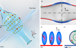
Scientists all over the world have since endeavored to achieve super-resolution imaging that capture the finest of details contained in evanescent waves that would otherwise be lost with conventional lenses. Hyperlenses are super-resolution devices that transform scattered evanescent waves into propagating waves to project the image into the far-field. Recent experiments that focus on a single hyperlens made from an anisotropic metamaterial with a hyperbolic dispersion have demonstrated far-field sub-diffraction imaging in real time. However, such devices are limited by an extremely small observation area which consequently require precise positioning of the subject. A hyperlens array has been considered to be a solution, but fabrication of such an array would be extremely difficult and prohibitively expensive with existing nanofabrication technologies.
Research conducted by Professor Junsuk Rho’s team from the Department of Mechanical Engineering and the Department of Chemical Engineering at Pohang University of Science and Technology in collaboration with research team from Korea University has made great contributions to overcoming this obstacle by demonstrating a scalable and reliable fabrication process of a large scale hyperlens device based on direct pattern transfer techniques. This achievement has been published in the world-renowned Scientific Reports.
The team solved the main limitations of previous fabrication methods of hyperlens devices through nanoimprint lithography. Based on a simple pattern transfer process, the team was able to readily fabricate a perfect large-scale hyperlens device on a replicated hexagonal array of hemisphere substrate directly printed and pattern-transferred from the master mold, followed by metal-dielectric multilayer deposition by electron beam evaporation. This 5 cm x 5 cm hyperlens array has been demonstrated to resolve sub-diffraction features down to 160 nm under a 410 nm wavelength visible light.
Professor Rho anticipates that the research team’s new cost-effective fabrication method can be used to proliferate practical far-field and real-time super-resolution imaging devices that can be widely used in optics, biology, medical science, nanotechnology, and other related interdisciplinary fields.