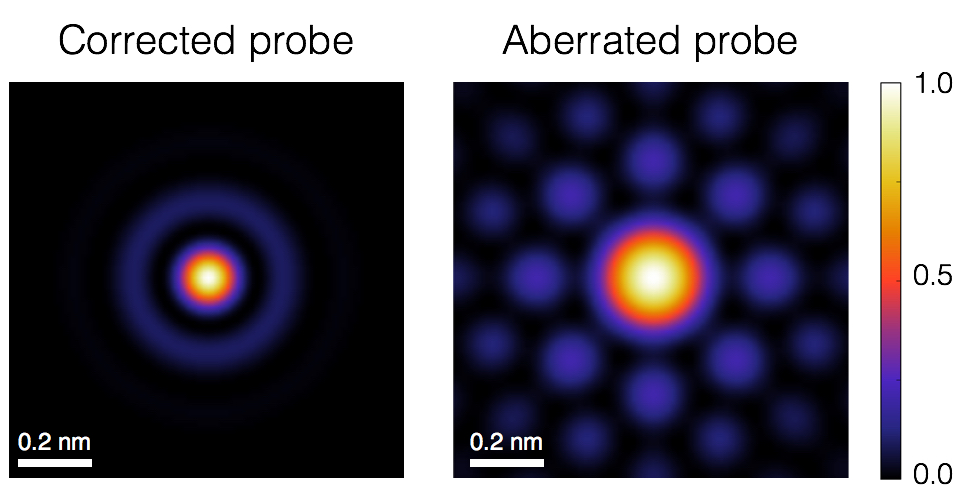
A new counterintuitive electron microscope approach can collect magnetic signals through the introduction of aberrations. The aberrated probe (right) results in imaging and spectra with lower spatial resolution than a traditionally corrected probe but can pick up a magnetic signature. (Credit: Oak Ridge National Laboratory)
Scientists can now detect magnetic behavior at the atomic level with a new electron microscopy technique developed by a team from the Department of Energy’s Oak Ridge National Laboratory and Uppsala University, Sweden. The researchers took a counterintuitive approach by taking advantage of optical distortions that they typically try to eliminate.
“It’s a new approach to measure magnetism at the atomic scale,” ORNL’s Juan Carlos Idrobo said. “We will be able to study materials in a new way. Hard drives, for instance, are made by magnetic domains, and those magnetic domains are about 10 nanometers apart.” One nanometer is a billionth of a meter, and the researchers plan to refine their technique to collect magnetic signals from individual atoms that are ten times smaller than a nanometer.
“If we can understand the interaction of those domains with atomic resolution, perhaps in the future we will able to decrease the size of magnetic hard drives,” Idrobo said. “We won’t know without looking at it.”
Researchers have traditionally used scanning transmission electron microscopes to determine where atoms are located within materials. This new technique allows scientists to collect more information about how the atoms behave.
“Magnetism has its origins at the atomic scale, but the techniques that we use to measure it usually have spatial resolutions that are way larger than one atom,” Idrobo said. “With an electron microscope, you can make the electron probe as small as possible and if you know how to control the probe, you can pick up a magnetic signature.”
The ORNL-Uppsala team developed the technique by rethinking a cornerstone of electron microscopy known as aberration correction. Researchers have spent decades working to eliminate different kinds of aberrations, which are distortions that arise in the electron-optical lens and blur the resulting images.
Instead of fully eliminating the aberrations in the electron microscope, the researchers purposely added a type of aberration, called four-fold astigmatism, to collect atomic level magnetic signals from a lanthanum manganese arsenic oxide material. The experimental study validates the team’s theoretical predictions presented in a 2014 Physical Review Letters study.

ORNL’s Juan Carlos Idrobo helped develop an electron microscopy technique to measure magnetism at the atomic scale. (Credit: ORNL)
“This is the first time someone has used aberrations to detect magnetic order in materials in electron microscopy,” Idrobo said. “Aberration correction allows you to make the electron probe small enough to do the measurement, but at the same time we needed to put in a specific aberration, which is opposite of what people usually do.”
Idrobo adds that new electron microscopy techniques can complement existing methods, such as x-ray spectroscopy and neutron scattering, that are the gold standard in studying magnetism but are limited in their spatial resolution.
The study is published as “Detecting magnetic ordering with atomic size electron probes,” in the journal of Advanced Structural and Chemical Imaging.