Much like an overcooked dinner, the next so-called wonder material for next-generation electronics has been “stuck to the pan” until researchers at the University of Wollongong’s Institute for Superconducting and Electronic Materials (ISEM) came up with a breakthrough solution.
The material is silicene, the thinnest possible form of silicon, comprised of a two-dimensional layer of silicon crystals.
Electrons move ultrafast in silicene, reducing the energy required to drive electronic devices and paving the way for even smaller, flexible, transparent, and low-energy-cost electronics.
Until now, silicene has been “grown” on a metal surface, but researchers had no proven way of freeing it from the substrate to create a freestanding material that could then be incorporated into electronic devices and components.
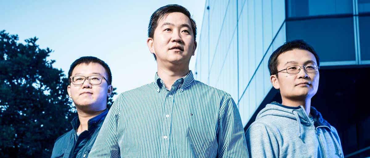
Dr. Zhi Li, Dr. Yi Du, and Dr. Jincheng Zhuang have been working on “oxygen scissors” to make freestanding silicene.
ISEM Research Fellow Dr. Yi Du and his team have used oxygen to separate a single-atom thick layer of silicon from its surface, overcoming the key hurdle preventing the production of a material with potential to supercharge electronics.
“We know silicene crystals prefer to firmly attach on the metallic substrate and because they are too thin to be peeled off by any mechanical tools, it’s impossible to remove them from the substrate,” Du says.
Researchers have experimented with the idea of using “chemical scissors” to break the bond between silicene and the substrate and the breakthrough for Du and his team came through using oxygen molecules as chemical scissors to cut the silicene from its substrate.
The work, supported by the Australian Research Council (ARC), involves several special techniques that can be done only at ISEM with the help of its powerful tools, including a scanning tunneling microscope, which creates an ultra-high vacuum environment about a hundred times higher than the vacuum level experienced in orbit at the International Space Station.
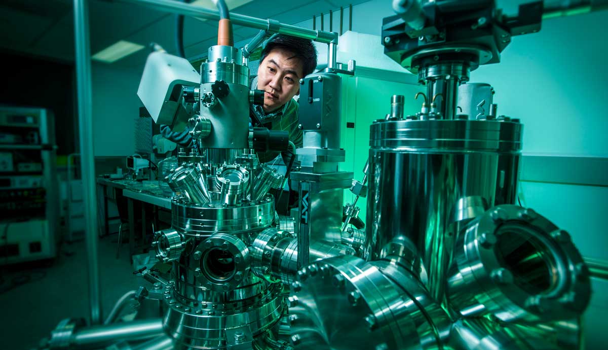
ISEM’s scanning tunneling microscope creates an ultra-high vacuum environment about a hundred times higher than the level experienced in orbit at the International Space Station.
“Because the vacuum levels are so high, we can inject the oxygen molecules into the chamber and they become a ‘molecular flux’ that follows a straight pathway,” Du says.
“This allows us to direct these molecules precisely into the silicene layers, acting like scissors to separate the silicene.”
The result is a layer of freestanding silicene — with an appearance much like a honeycomb lattice — that could be transferred to an insulating substrate to make advanced transistors.
The theory for two-dimensional silicene was introduced in 1994 but it wasn’t until 2012 that scientists, including a team at UOW, successfully fabricated silicene in the lab.
Silicene is emerging player in the super-materials category, alongside graphene, which is a single-atom thick layer of carbon.
Graphene has been shown to be the fastest conductor of electricity yet found, faster than commonly used silicon. Graphene can’t be switched between on and off states of conductivity.
This makes it unsuitable for applications such as transistors. Because silicon and carbon sit side-by-side on the periodic table, scientists were inspired to investigate if silicon’s atomic properties could be similarly revolutionary but more easily exploited because of its compatibility with existing silicon-based electronics.
“This work solves the long-lasting problem of isolating this super material for further device development. It challenges the entire scientific literature on silicene since its discovery,” Du says.
“These findings are relevant for the future design and application of silicene-based nano-electronic and spintronic devices.”
The research was published recently in the journals Science Advances and ACS Central Science and is the result of collaboration between Australian and Chinese researchers including Professor Jijun Zhao, from the Dalian University of Technology and Dr. Jiaou Wang at the Beijing Synchrotron Radiation Facility (Chinese Academy of Sciences).
This research was supported under Australian Research Council’s Discovery Projects funding scheme.
Source: University of Wollongong