Stress induced deformation observed during the application of pressure and after the pressure has been released. Image courtesy of the MIPT press office.
Researchers from the Moscow Institute of Physics and Technology (MIPT), Technological Institute for Superhard and Novel Carbon Materials (TISNCM), Lomonosov Moscow State University (MSU), and the National University of Science and Technology MISiS have shown that an ultrastrong material can be produced by “fusing” multiwall carbon nanotubes together. The research findings have been published in Applied Physics Letters.
According to the scientists, a material of that kind is strong enough to endure very harsh conditions, making it useful for applications in the aerospace industry, among others.
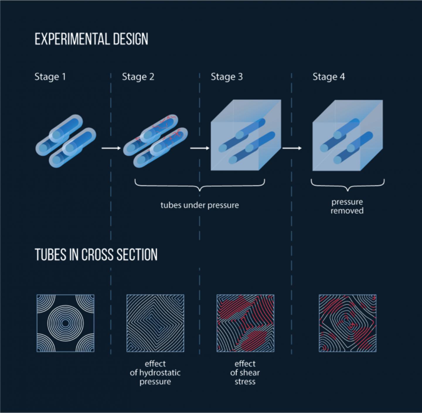
The authors of the paper performed a series of experiments to study the effect of high pressure on multiwall carbon nanotubes (MWCNTs). In addition, they simulated nanotube behavior in high pressure cells, finding that the shear stress strain in the outer walls of the MWCNTs causes them to connect to each other as a result of the structural rearrangements on their outer surfaces. The inner concentric nanotubes, however, retain their structure completely: they simply shrink under pressure and restore their shape once the pressure is released.
The main feature of this study is that it demonstrates the possibility of covalent intertube bonding giving rise to interconnected (polymerized) multiwall nanotubes; these nanotubes being cheaper to produce than their single-wall counterparts.
“These connections between the nanotubes only affect the structure of the outer walls, whereas the inner layers remain intact. This allows us to retain the remarkable durability of the original nanotubes,” comments Prof. Mikhail Y. Popov of the Department of Molecular and Chemical Physics at MIPT, who heads the Laboratory of Functional Nanomaterials at TISNCM.
A shear diamond anvil cell (SDAC) was used for the pressure treatment of the nanotubes. The experiments were performed at pressures of up to 55 GPa, which is 500 times the water pressure at the bottom of the Mariana Trench. The cell consists of two diamonds, between which samples of a material can be compressed. The SDAC is different from other cell types in that it can apply a controlled shear deformation to the material by rotating one of the anvils. The sample in an SDAC is thus subjected to pressure that has both a hydrostatic and a shear component, i.e., the stress is applied both at a normal and parallel to its surface. Using computer simulations, the scientists found that these two types of stress affect the structure of the tubes in different ways. The hydrostatic pressure component alters the geometry of the nanotube walls in a complex manner, whereas the shear stress component induces the formation of sp³-hybridized amorphized regions on the outer walls, connecting them to the neighboring carbon tubes by means of covalent bonding. When the stress is removed, the shape of the inner layers of the connected multiwall tubes is restored.
Carbon nanotubes have a wide range of commercial applications by virtue of their unique mechanical, thermal and conduction properties. They are used in batteries and accumulators, tablet and smartphone touch screens, solar cells, antistatic coatings, and composite frames in electronics.


