
Quantum Twins illustration showing thousands of quantum dots patterned with atomic precision on pure silicon. (Image: Silicon Quantum Computing)
Silicon Quantum Computing has built what is, in effect, a designer material you can dial like an instrument.
Using scanning tunneling microscope lithography, the Sydney-based company patterned a two-dimensional lattice of roughly 15,000 atom-based quantum dots in silicon, arranged on a 100×150 grid. Results published in Nature show controlled simulation of quantum physics across arrays roughly 1,500 times larger than previous attempts with this approach.
The team operated the device as an analog quantum simulator. They tuned the balance between electron hopping and on-site Coulomb repulsion. Next, they observed the 2D lattice switch from conducting to insulating, a metal-insulator transition central to strongly correlated electron physics and relevant to models of unconventional superconductivity.
Each site is a quantum dot containing roughly 50 phosphorus donor atoms embedded in isotopically purified silicon. SQC claims 0.13 nm placement accuracy: one atomic width. The researchers built separate arrays. The center-to-center spacings ranged from 7.2 nm to 15.5 nm. That span shifts the tunneling energy scale by more than a factor of ten while holding electron-electron interaction strength relatively constant and large.

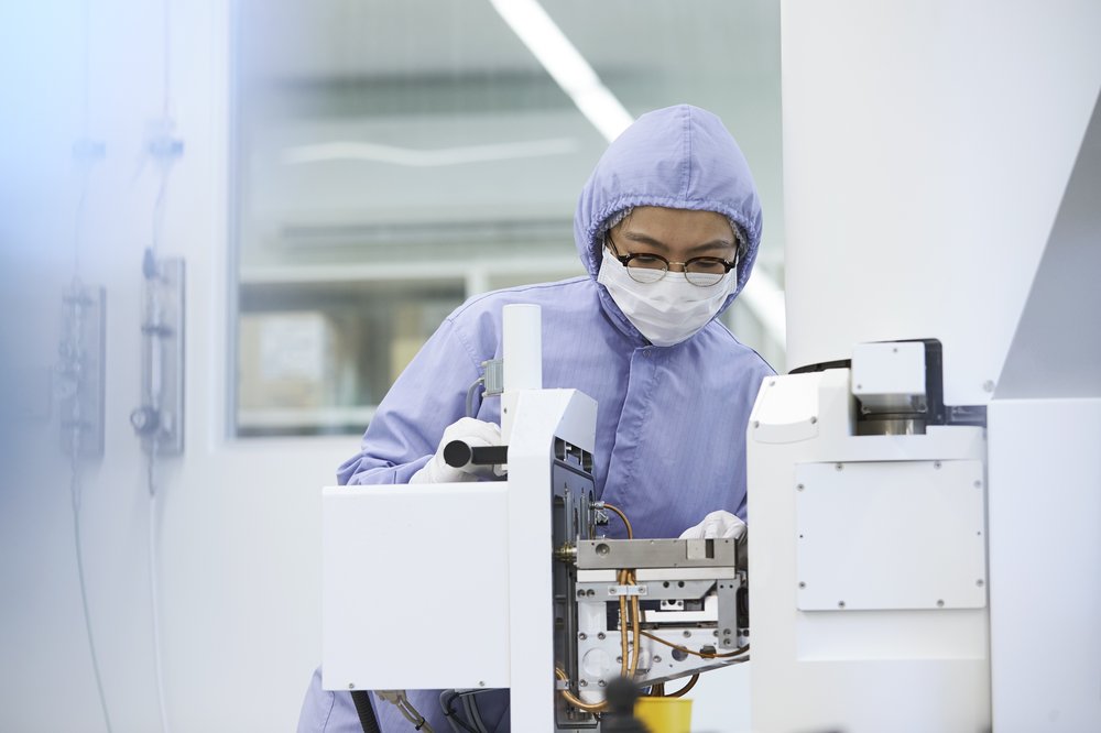
Michelle Simmons, founder and CEO of Silicon Quantum Computing. (Image: Silicon Quantum Computing)The key ratio governing correlated behavior, interaction strength divided by tunneling, could be swept from about 14 up past 200, letting the device function like a knobbed version of a strongly correlated material.
“The enabler is that we can engineer hundreds of thousands of qubit registers with atomic precision,” said CEO Michelle Simmons. “It’s an incredible achievement in semiconductor manufacturing with sub-nanometer accuracy.”
One difficulty with quantum materials is that when interactions dominate, classical simulation methods hit well-known roadblocks, including exponential scaling and sign problems for fermionic models. An analog quantum simulator sidesteps that by letting nature do the bookkeeping: physically build a clean, controllable version of the system and measure its behavior directly.
The authors make that pitch, writing that these precision-engineered simulators “provide a unique platform to simulate quantum materials on arbitrary two-dimensional lattices and to explore many unanswered questions in the formation of quantum magnetism, interacting topological quantum matter and unconventional superconductivity.”
What has been missing in solid-state platforms is a combination of scale, uniformity and a tunable path across regimes that includes the metal-insulator boundary. This work addresses all three.
What it is not
This is not a fault-tolerant, gate-based quantum computer executing long circuits. It is a purpose-built physical simulator for a class of problems. The right comparison is other analog simulators, cold atom arrays, twisted moire materials, not IBM or Google superconducting processors running Shor’s algorithm.
That said, SQC does position its broader silicon qubit platform against superconducting and ion trap approaches. The company points to benchmark results on Grover’s search algorithm: 98.9% fidelity for its qubits versus 96% for ion trap and 81% for superconducting systems, according to company data.
A researcher prepares silicon wafers for atomic-scale patterning at SQC’s Sydney facility. (Image: Silicon Quantum Computing)
Commercial trajectory
SQC has launched the simulator technology as Quantum Twins, marketing custom chips that physically encode analogs of a customer’s target quantum system for materials and chemistry applications. The company’s quantum machine learning product, Watermelon, has been trialed with Australian telecom Telstra.
On manufacturing, SQC says its in-house fabrication line can iterate chips in one to two weeks, compared to what the company estimates as 17–40 weeks for competitors relying on external foundries. The company says it patterned 250,000 qubit registers in eight hours in November 2025.
SQC recently advanced to Stage B of DARPA’s Quantum Benchmarking Initiative, which evaluates paths to utility-scale quantum computing by 2033—the same year SQC targets for a commercial-scale, fault-tolerant system.
“Expanding our product offering with the launch of Quantum Twins brings SQC’s atomic-scale advantage to the global materials and chemistry sectors,” said chair Simon Segars, former CEO of ARM.


Tell Us What You Think!
You must be logged in to post a comment.