Research & Development World

  • R&D World Home
  • Topics
    • Aerospace
    • Automotive
    • Biotech
    • Careers
    • Chemistry
    • Environment
    • Energy
    • Life Science
    • Material Science
    • R&D Management
    • Physics
  • Technology
    • 3D Printing
    • A.I./Robotics
    • Software
    • Battery Technology
    • Controlled Environments
      • Cleanrooms
      • Graphene
      • Lasers
      • Regulations/Standards
      • Sensors
    • Imaging
    • Nanotechnology
    • Scientific Computing
      • Big Data
      • HPC/Supercomputing
      • Informatics
      • Security
    • Semiconductors
  • R&D Market Pulse
  • R&D 100
    • 2025 R&D 100 Award Winners
    • 2025 Professional Award Winners
    • 2025 Special Recognition Winners
    • R&D 100 Awards Event
    • R&D 100 Submissions
    • Winner Archive
  • Resources
    • Research Reports
    • Digital Issues
    • Educational Assets
    • Subscribe
    • Video
    • Webinars
    • PharmSci360
    • Content submission guidelines for R&D World
  • Global Funding Forecast
  • Top Labs
  • Advertise
  • SUBSCRIBE

Researchers Invent Light-Emitting Nanoantennas

By ITMO University | February 22, 2018

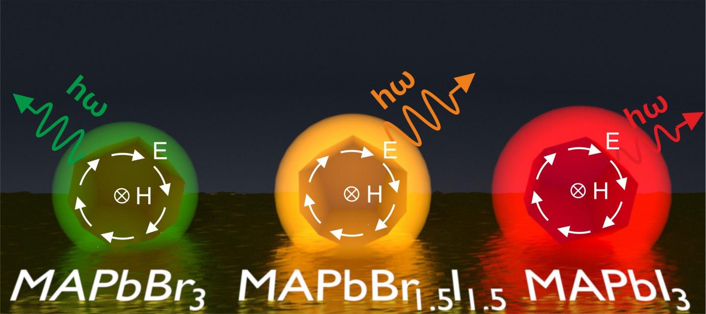
Nanoantennas obtained by the scientists change their emiison wavelength depenging on the material composition.

Nanoscale light sources and nanoantennas already found a wide range of applications in several areas, such as ultra compact pixels, optical detection or telecommunications. However, the fabrication of nanostructure-based devices is rather complicated since the materials typically used have a limited luminescence efficiency. What is more, single quantum dots or molecules usually emit light non-directionally and weakly. An even more challenging task is placing a nanoscale light source precisely near a nanoantenna.

A research group from ITMO University managed to combine a nanoantenna and a light source in a single nanoparticle. It can generate, enhance and route emission via excited resonant modes coupled with excitons. “We used hybrid perovskite as a material for such nanoantennas,” says Ekaterina Tiguntseva, first author of the publication. “Unique features of perovskite enabled us to make nanoantennas from this material. We basically synthesized perovskite films, and then transferred material particles from the film surface to another substrate by means of pulsed laser ablation technique. Compared to alternatives, our method is relatively simple and cost-effective.”

While studying the obtained perovskite nanoparticles, the scientists discovered that their emission can be enhanced if its spectra match with the Mie-resonant mode. “Currently, scientists are particularly interested in Mie-resonances related to dielectric and semiconductor nanoparticles,” explains George Zograf, Engineer at the Laboratory of Hybrid Nanophotonics and Optoelectronics at ITMO University. “Perovskites used in our work are semiconductors with luminescence efficiency much higher than that of many other materials. Our study shows that combination of excitons with Mie resonance in perovskite nanoparticles makes them efficient light sources at room temperature.”

In addition, the radiation spectrum of the nanoparticles can be changed by varying the anions in the material. “The structure of the material remains the same, we simply use another component in the synthesis of perovskite films. Therefore, it is not necessary to adjust the method each time. It remains the same, yet the emission color of our nanoparticles changes,” says Ekaterina.

The scientists will continue research on light-emitting perovskite nanoantennas using various components for their synthesis. In addition, they are developing new designs of perovskite nanostructures which may improve ultra compact optical devices.

###
Related Articles Read More >

Researchers developed quantum nanosensors that can measure the temperature of a single cell
Overcoming the 100-nanometer barrier: New microbottle resonators scale up optical trapping
R&D 100 winner LLNL achieves 1,000x speed boost in 3D nanofabrication
CEA-Leti achieves 400°C CMOS fabrication milestone for 3D chip stacking
rd newsletter
EXPAND YOUR KNOWLEDGE AND STAY CONNECTED
Get the latest info on technologies, trends, and strategies in Research & Development.

R&D World Digital Issues

Fall 2025 issue

Browse the most current issue of R&D World and back issues in an easy to use high quality format. Clip, share and download with the leading R&D magazine today.

R&D 100 Awards
Research & Development World
  • Subscribe to R&D World Magazine
  • Sign up for R&D World’s newsletter
  • Contact Us
  • About Us
  • Drug Discovery & Development
  • Pharmaceutical Processing
  • Global Funding Forecast

Copyright © 2026 Arrowfly LLC. All Rights Reserved. The material on this site may not be reproduced, distributed, transmitted, cached or otherwise used, except with the prior written permission of Arrowfly
Privacy Policy | Advertising | About Us

Search R&D World

  • R&D World Home
  • Topics
    • Aerospace
    • Automotive
    • Biotech
    • Careers
    • Chemistry
    • Environment
    • Energy
    • Life Science
    • Material Science
    • R&D Management
    • Physics
  • Technology
    • 3D Printing
    • A.I./Robotics
    • Software
    • Battery Technology
    • Controlled Environments
      • Cleanrooms
      • Graphene
      • Lasers
      • Regulations/Standards
      • Sensors
    • Imaging
    • Nanotechnology
    • Scientific Computing
      • Big Data
      • HPC/Supercomputing
      • Informatics
      • Security
    • Semiconductors
  • R&D Market Pulse
  • R&D 100
    • 2025 R&D 100 Award Winners
    • 2025 Professional Award Winners
    • 2025 Special Recognition Winners
    • R&D 100 Awards Event
    • R&D 100 Submissions
    • Winner Archive
  • Resources
    • Research Reports
    • Digital Issues
    • Educational Assets
    • Subscribe
    • Video
    • Webinars
    • PharmSci360
    • Content submission guidelines for R&D World
  • Global Funding Forecast
  • Top Labs
  • Advertise
  • SUBSCRIBE