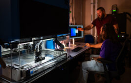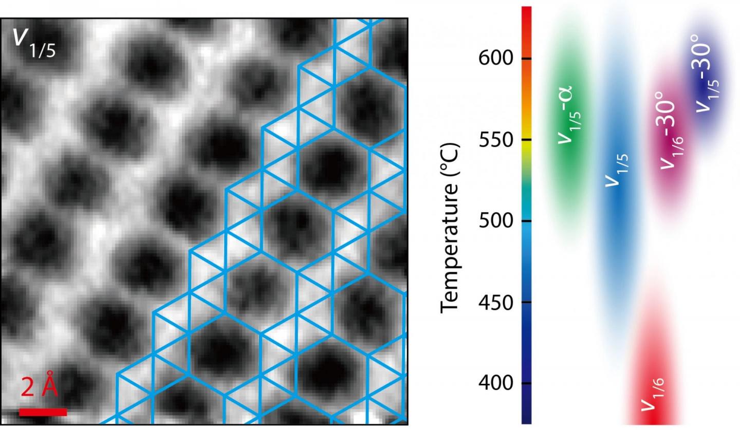
Scientists at Rice and Northwestern universities have developed a technique to get images of two-dimensional borophene and match them with models. Polymorphic borophene shows promise for electronic, thermal, optical and other applications. The researchers also created a phase diagram, at right, with details about borophene polymorphs observed to date. Credit: Xiaolong Liu/Northwestern University
Graphene can come from graphite. But borophene? There’s no such thing as borite.
Unlike its carbon cousin, two-dimensional borophene can’t be reduced from a larger natural form. Bulk boron is usually only found in combination with other elements, and is certainly not layered, so borophene has to be made from the atoms up. Even then, the borophene you get may not be what you need.
For that reason, researchers at Rice and Northwestern universities have developed a method to view 2D borophene crystals, which can have many lattice configurations — called polymorphs — that in turn determine their characteristics.
Knowing how to achieve specific polymorphs could help manufacturers incorporate borophene with desirable electronic, thermal, optical and other physical properties into products.
Boris Yakobson, a materials physicist at Rice’s Brown School of Engineering, and materials scientist Mark Hersam of Northwestern led a team that not only discovered how to see the nanoscale structures of borophene lattices but also built theoretical models that helped characterize the crystalline forms.
Their results are published in Nature Communications.
Borophene remains hard to make in even small quantities. If and when it can be scaled up, manufacturers will likely want to fine-tune it for applications. What the Rice and Northwestern teams learned will help in that regard.
Graphene takes a single form – an array of hexagons, like chicken wire – but perfect borophene is a grid of triangles. However, borophene is a polymorph, a material that can have more than one crystal structure. Vacancies that leave patterns of “hollow hexagons” in a borophene lattice determine its physical and electrical properties.
Yakobson said there could theoretically be more than 1,000 forms of borophene, each with unique characteristics.
“It has many possible patterns and networks of atoms being connected in the lattice,” he said.
The project started at Hersam’s Northwestern lab, where researchers modified the blunt tip of an atomic force microscope with a sharp tip of carbon and oxygen atoms. That gave them the ability to scan a flake of borophene to sense electrons that correspond to covalent bonds between boron atoms. They used a similarly modified scanning tunneling microscope to find hollow hexagons where a boron atom had gone missing.
Scanning flakes grown on silver substrates under various temperatures via molecular-beam epitaxy showed them a range of crystal structures, as the changing growth conditions altered the lattice.
“Modern microscopy is very sophisticated, but the result is, unfortunately, that the image you get is generally difficult to interpret,” Yakobson said. “That is, it’s hard to say an image corresponds to a particular atomic lattice. It’s far from obvious, but that’s where theory and simulations come in.”
Yakobson’s team used first-principle simulations to determine why borophene took on particular structures based on calculating the interacting energies of both boron and substrate atoms. Their models matched many of the borophene images produced at Northwestern.
“We learned from the simulations that the degree of charge transfer from the metal substrate into borophene is important,” he said. “How much of this is happening, from nothing to a lot, can make a difference.”
The researchers confirmed through their analysis that borophene is also not an epitaxial film. In other words, the atomic arrangement of the substrate doesn’t dictate the arrangement or rotational angle of borophene.
The team produced a phase diagram that lays out how borophene is likely to form under certain temperatures and on a variety of substrates, and noted their microscopy advances will be valuable for finding the atomic structures of emerging 2D materials.
Looking to the future, Hersam said, “The development of methods to characterize and control the atomic structure of borophene is an important step toward realizing the many proposed applications of this material, which range from flexible electronics to emerging topics in quantum information sciences.”