Researchers at the University of Pennsylvania’s School of Engineering and Applied Science have now demonstrated a new hardware platform based on isolated electron spins in a two-dimensional material. The electrons are trapped by defects in sheets of hexagonal boron nitride, a one-atom-thick semiconductor material, and the researchers were able to optically detect the system’s quantum states. Image: Ann Sizemore Blevins
Quantum computers promise to be a revolutionary technology because their elementary building blocks, qubits, can hold more information than the binary, 0-or-1 bits of classical computers. But to harness this capability, hardware must be developed that can access, measure and manipulate individual quantum states.
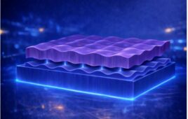
Researchers at the University of Pennsylvania’s School of Engineering and Applied Science have now demonstrated a new hardware platform based on isolated electron spins in a two-dimensional material. The electrons are trapped by defects in sheets of hexagonal boron nitride, a one-atom-thick semiconductor material, and the researchers were able to optically detect the system’s quantum states.
The study was led by Lee Bassett, assistant professor in the Department of Electrical and Systems Engineering, and Annemarie Exarhos, then a postdoctoral researcher in his lab.
Fellow Bassett Lab members David Hopper and Raj Patel, along with Marcus Doherty of the Australian National University, also contributed to the study.
It was published in the journal Nature Communications, where it was selected as an Editor’s Highlight.
There are number of potential architectures for building quantum technology. One promising system involves electron spins in diamonds: these spins are also trapped at defects in diamond’s regular crystalline pattern where carbon atoms are missing or replaced by other elements. The defects act like isolated atoms or molecules, and they interact with light in a way that enables their spin to be measured and used as a qubit.
These systems are attractive for quantum technology because they can operate at room temperatures, unlike other prototypes based on ultra-cold superconductors or ions trapped in vacuum, but working with bulk diamond presents its own challenges.
“One disadvantage of using spins in 3-D materials is that we can’t control exactly where they are relative to the surface” Bassett says. “Having that level of atomic scale control is one reason to work in 2-D. Maybe you want to place one spin here and one spin there and have them talk them to each other. Or if you want to have a spin in a layer of one material and plop a 2-D magnet layer on top and have them interact. When the spins are confined to a single atomic plane, you enable a host of new functionalities.”
With nanotechnological advances producing an expanding library of 2-D materials to choose from, Bassett and his colleagues sought the one that would be most like a flat analog of bulk diamond.
“You might think the analog would be graphene, which is just a honeycomb lattice of carbon atoms, but here we care more about the electronic properties of the crystal than what type of atoms it’s made of,” says Exarhos, who is now an assistant professor of Physics at Lafayette University. “Graphene behaves like a metal, whereas diamond is a wide-bandgap semiconductor and thus acts like an insulator. Hexagonal boron nitride, on the other hand, has the same honeycomb structure as graphene, but, like diamond, it is also a wide-bandgap semiconductor and is already widely used as a dielectric layer in 2-D electronics.”
With hexagonal boron nitride, or h-BN, widely available and well characterized, Bassett and his colleagues focused on one of its less well-understood aspects: defects in its honeycomb lattice that can emit light.
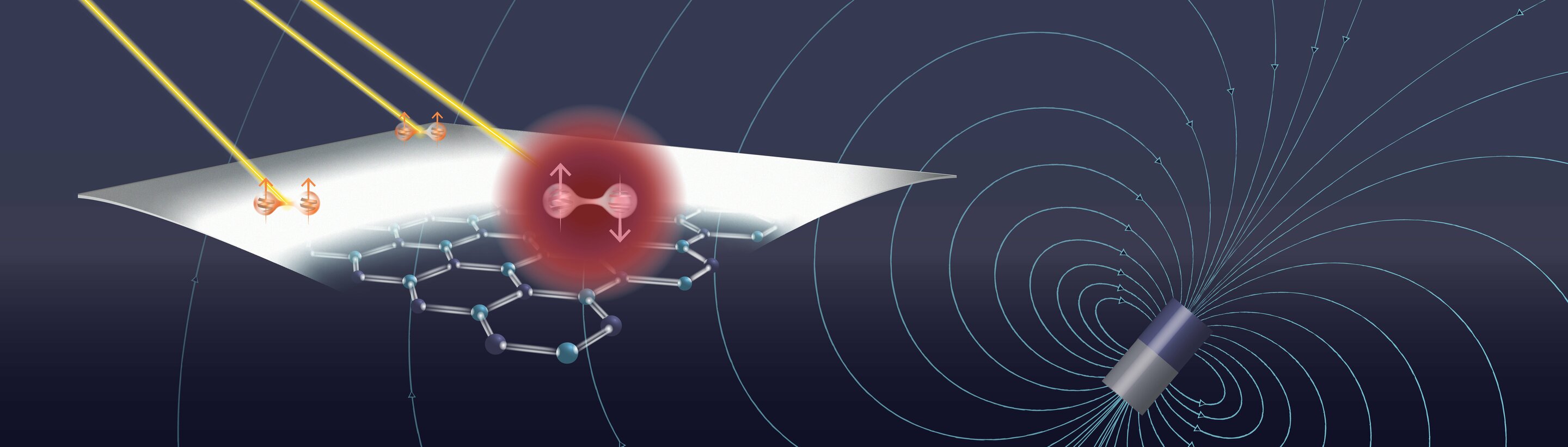
That the average piece of h-BN contains defects that emit light had previously been known. Bassett’s group is the first to show that, for some of those defects, the intensity of the emitted light changes in response to a magnetic field.
“We shine light of one color on the material and we get photons of another color back,” Bassett says. “The magnet controls the spin and the spin controls the number of photons that the defects in the h-BN emit. That’s a signal that you can potentially use as a qubit.”
Beyond computation, having the building block of a quantum machine’s qubits on a 2-D surface enables other potential applications that depend on proximity.
“Quantum systems are super sensitive to their environments, which is why they’re so hard to isolate and control,” Bassett says. “But the flip side is that you can use that sensitivity to make new types of sensors. In principle, these little spins can be miniature nuclear magnetic resonance detectors, like the kind used in MRIs, but with the ability to operate on a single molecule.
Nuclear magnetic resonance is currently used to learn about molecular structure, but it requires millions or billions of the target molecule to be assembled into a crystal. In contrast, 2-D quantum sensors could measure the structure and internal dynamics of individual molecules, for example to study chemical reactions and protein folding.
While the researchers conducted an extensive survey of h-BN defects to discover ones that have special spin-dependent optical properties, the exact nature of those defects is still unknown. Next steps for the team include understanding what makes some, but not all, defects responsive to magnetic fields, and then recreating those useful defects.
Some of that work will be enabled by Penn’s Singh Center for Nanotechnology and its new JEOL NEOARM microscope. The only transmission electron microscope of its kind in the United States, the NEOARM is capable of resolving single atoms and potentially even creating the kinds of defects the researchers want to work with.
“This study is bringing together two major areas of scientific research,” Bassett says. “On one hand, there’s been a tremendous amount of work in expanding the library of 2-D materials and understanding the physics that they exhibit and the devices they can make. On the other hand, there’s the development of these different quantum architectures. And this is one of the first to bring them together to say ‘here’s a potentially room-temperature quantum architecture in a 2-D material.'”