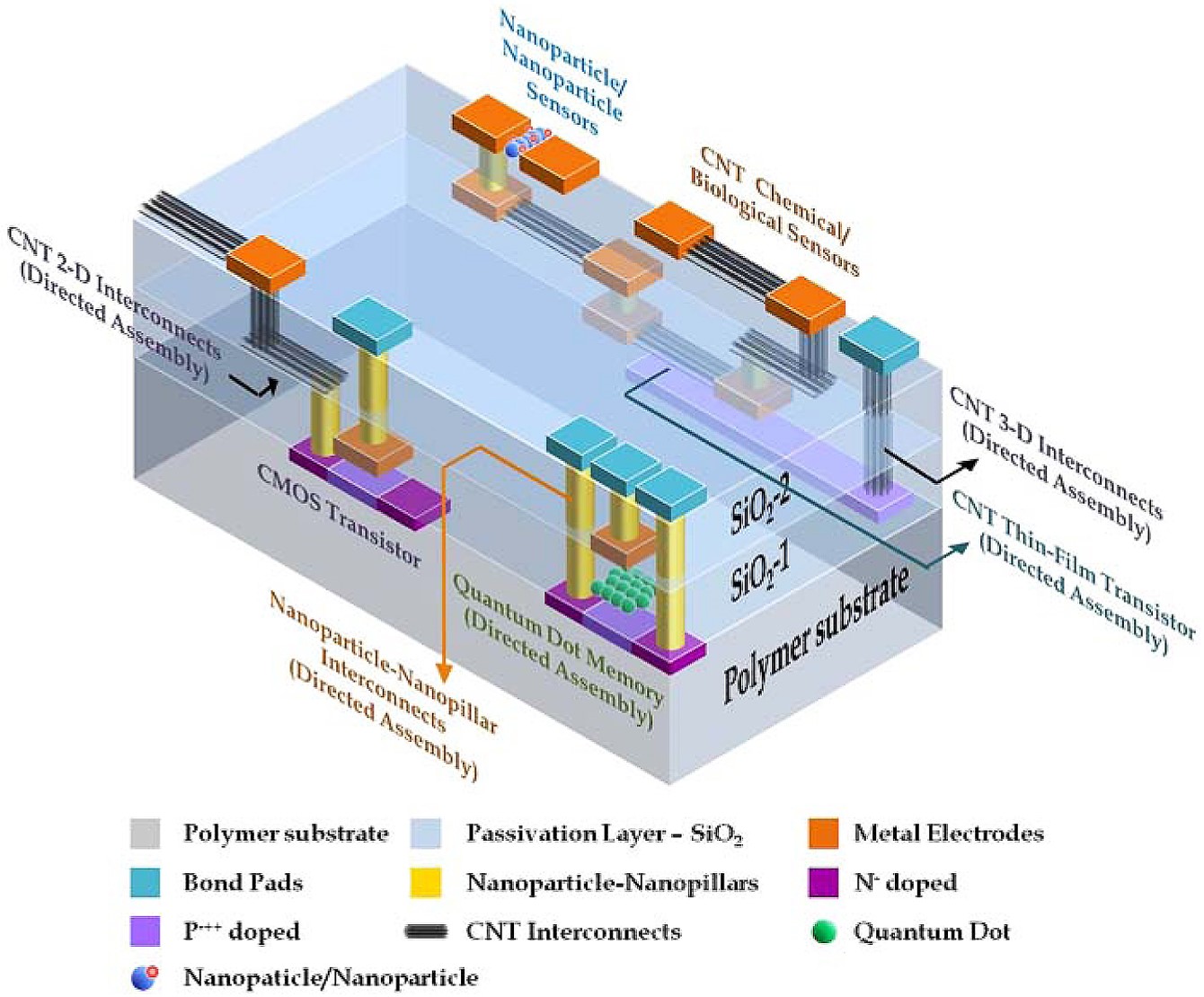
A chip with nanoscale features and functionality using a variety nanomaterials.
Over the past two decades the cost of commercial electronics manufacturing has continued to increase, with some fabrication facilities costing billions—Taiwan Semiconductor Manufacturing Company announced last year that their next plant will cost $20 billion—and requiring massive quantities of water and power. This high cost of entry barrier shuts out small and medium size businesses.
Conventional nanofabrication technologies—although responsible for all of the technological progress we’ve experienced during the last three decades—have not been able to take advantage of many of the novel and superior properties of nanomaterials. These include 0D nanomaterials (e.g., quantum dots, other conductive, semiconducting, or insulating nanoparticles); 1D nanomaterials (e.g., carbon nanotubes or nanowires); 2D nanomaterials (e.g., molybdenum disulfide [MoS2], graphene, etc.) that were discovered during the last two decades. There is a need to have the capability to build a circuit that uses many of these nanomaterials with different semiconductors and conductors (organic or inorganic) on the same chip.
The Internet of Things (IoT) or Industry 4.0 is the network of physical objects embedded with sensors, electronics, software and connectivity. IoT has a total potential impact of up to $11 trillion per year by 2025, and will affect every industry and community on earth. However, these IoT market projections can only succeed if low cost ubiquitous sensors and electronics are made available. Printing of electronics offers significant savings over similar conventional silicon or gallium nitride based electronics fabrication.
Over the past decade, there has been a paradigm shift in manufacturing of low-end electronic devices away from conventional fabrication processes and toward printing technologies. Inkjet, screen-printing, and gravure printing are technologies that are commercially used for printing electronics, flexible displays, and RFID tags. However, currently only the RFID antennas and interconnects are printed; the chips are made using conventional fabrication. For example, the cost of a printed integrated sensor device is 10-100 times less than the cost of current silicon-based systems. Current printing, however, scale-wise is 40 years old. Printed features using inkjets is about 20 microns, which was silicon electronics’ line width in 1975.
The next generation of printed devices requires a technology leap to print features at today’s silicon electronics line width, which is 20 nm or less—some 1000 times smaller than current inkjet capability. There is a need for a nanoscale high-throughput printing technology that is high-rate, that can utilize a variety of nanomaterials, and that is capable of printing heterogeneous structures.
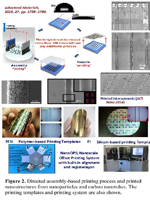
The directed assembly-based printing processes, developed by the NSF Science and Engineering Center for High-rate Nanomanufacturing (CHN) at Northeastern University, meets these requirements. The processes were specifically developed to be scalable, high-throughput, sustainable, yet show precise and repeatable control printing of various nanomaterials. The high-rate offset nanoscale printing technology using reusable Damascene templates utilizing electrophoretic directed assembly (for inking) and transfer (printing) processes, as shown in Figure 2. These efforts have resulted in over 50 patent applications (20 granted to date) that cover the directed assembly-based printing and printed devices.
The technology has used these processes to print ordered arrays and networks of nanoparticle, conducting polymers, polymer blends, 2D materials and SWNTs into various non-uniform structures including three dimensional architecture at multiple length scales that are patterned on rigid or compliant substrates and transferring them. Using these individual processes, various novel nanomaterial based device components such as transistors, chemical and biosensors, and interconnects have been fabricated, including 2D materials (MoS2) transistors and inverters. In 2014, Northeastern CHN unveiled the first fully automated Nanoscale Offset Printing System (NanoOPS) shown at the bottom of Figure 2. NanoOPS is designed to print devices and products down to 20 nm or smaller using conductive, semiconducting or insulating, organic or inorganic materials. The printing process is much faster than current 3D or inkjet based electronic printing systems, regardless of the pattern scale or density.
In 2014, in collaboration with Milara, Inc., a Boston automation company, the world’s first nanoscale fully automated offset printing system (NanoOPS) for 3D printing of sensors and electronics. NanoOPS is fast, scalable, and capable of printing multiscale (nano, micro and macro) structures at low facilities and operational cost. It is fully automated, robotic, and cyber-enabled. It is three orders of magnitude faster and higher resolution than the current inkjet and 3D printing. The printing process takes place at room temperature and pressure, and the ink can include variety of nanomaterials (nanoparticles, nanotubes, or polymers) suspended mostly in water. Any material that can be suspended or dissolved in a liquid can be printed on any flexible or rigid substrate. Nano OPS can print 1000 times faster and 1000 times smaller circuit lines, than inkjet or 3D printer at a cost that’s 10-100 times less than conventional nanofabrication. The second generation of Nano OPS (NanoOPS Gen 2) was unveiled on December 13, 2017. The Third Generation NanoOPS is scheduled to be unveiled in the summer of 2018.
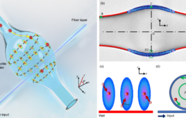
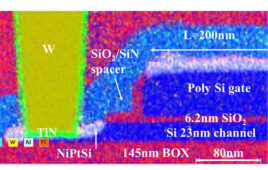
The technology has been used to print transistors and diodes using a variety of organic and inorganic semiconductors. It has been used to print nano and micro LEDs using inorganic semiconductors and a biosensor platform for real-time pathogen monitoring and for wearable sensors to monitor physiologic state, such as measuring glucose using sweat as shown in Figure 3. These printed flexible sensors were printed for wearable sensors that could be used as an electronic skin or for physiological monitoring as well as environmental monitoring.
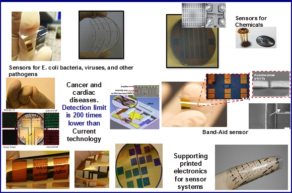
Figure 3. Examples of directed assembly-based printed sensors and electronics.
This printing technology can “democratize” nanomanufacturing, making it more broadly accessible to industry and entrepreneurs and unleashing a wave of creativity for nano-enabled product innovation. For example, a directed assembly-based printing manufacturing facility could be built for less than $50 million, a fraction of today’s cost, making nanotechnology accessible to millions of new innovators and entrepreneurs and unleash a wave of creativity the same way the advent of the PC has done for computing and the internet.
Videos sponsored by the National Science Foundation featured the printing technology are available: https://www.youtube.com/watch?v=2iEjIcog774 and the Museum of Science Boston documentary: https://www.youtube.com/watch?v=tZeO9I1KEec. For more info visit www.nano-ops.net
About the Author
Ahmed A. Busnaina is the William Lincoln Smith Professor, Distinguished University Professor and Director, the Advanced Nanomanufacturing Cluster for Smart Sensors and Materials CSSM, the NSF Nanoscale Science and Engineering Center for High-rate Nanomanufacturing, Northeastern University, Boston, MA “He is also the CTO of Nano OPS, Inc. www.nano-ops.net
For more info: www.nanomanufacturing.us