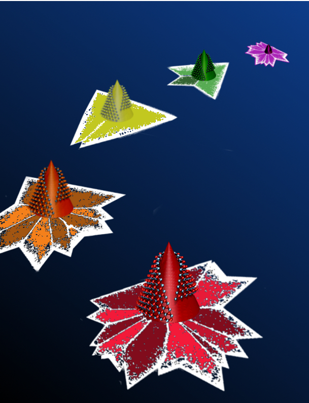
Researchers at Rice University and Oak Ridge National Laboratory determined that two-dimensional materials grown onto a cone allow control over where defects called grain boundaries appear. These defects can be used to enhance the materials’ electronic, mechanical, catalytic and optical properties. (Credit: Yakobson Research Group/Rice University)
Rice University researchers have learned to manipulate two-dimensional materials to design in defects that enhance the materials’ properties.
The Rice lab of theoretical physicist Boris Yakobson and colleagues at Oak Ridge National Laboratory are combining theory and experimentation to prove it’s possible to give 2-D materials specific defects, especially atomic-scale seams called grain boundaries. These boundaries may be used to enhance the materials’ electronic, magnetic, mechanical, catalytic and optical properties.
The key is introducing curvature to the landscape that constrains the way defects propagate. The researchers call this “tilt grain boundary topology,” and they achieve it by growing their materials onto a topographically curved substrate—in this case, a cone. The angle of the cone dictates if, what kind and where the boundaries appear.
The research is the subject of a paper in the American Chemical Society journal ACS Nano.
Grain boundaries are the borders that appear in a material where edges meet in a mismatch. These boundaries are a series of defects; for example, when two sheets of hexagonal graphene meet at an angle, the carbon atoms compensate for it by forming nonhexagonal (five- or seven-member) rings.
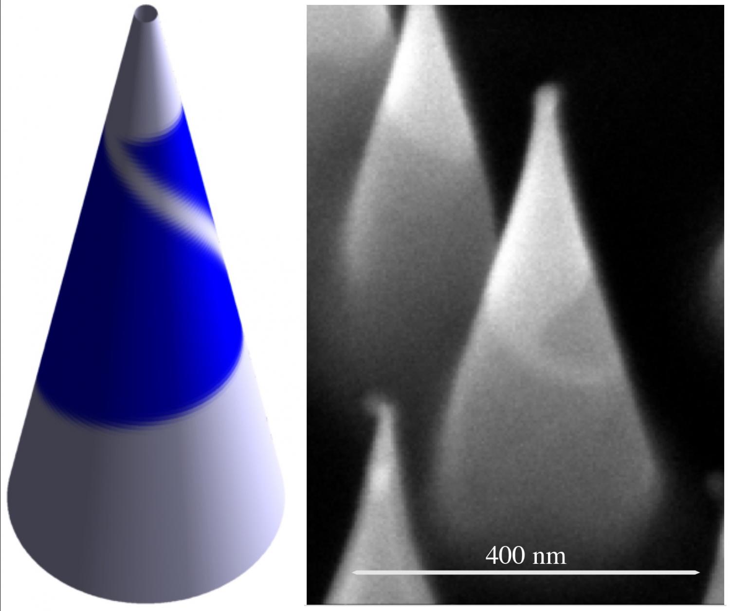
A theoretical model at left, created at Rice University, shows a triangular flake of tungsten disulfide grown around a cone that forces the creation of a grain boundary at a specific angle. The Rice researchers showed the width of the cone could be used to determine the placement of the boundary, and scientists at Oak Ridge National Laboratory proved it when they made the matching material seen in the electron microscope image at right. (Credit: Rice University/Oak Ridge National Laboratory)
Yakobson and his team have already demonstrated that these boundaries can be electronically significant. They can, for instance, turn perfectly conducting graphene into a semiconductor. In some cases, the boundary itself may be a conductive subnanoscale wire or take on magnetic properties.
But until now researchers had little control over where those boundaries would appear when growing graphene, molybdenum disulfide or other 2-D materials by chemical vapor deposition.
The theory developed at Rice showed growing 2-D material on a cone would force the boundaries to appear in certain places. The width of the cone controlled the placement and, more importantly, the tilt angle, a crucial parameter in tuning the materials’ electronic and magnetic properties, Yakobson said.
Experimental collaborators from Oak Ridge led by co-author David Geohegan provided evidence backing key aspects of the theory. They achieved this by growing tungsten disulfide onto small cones similar to those in Rice’s computer models. The boundaries that appeared in the real materials matched those predicted by theory.
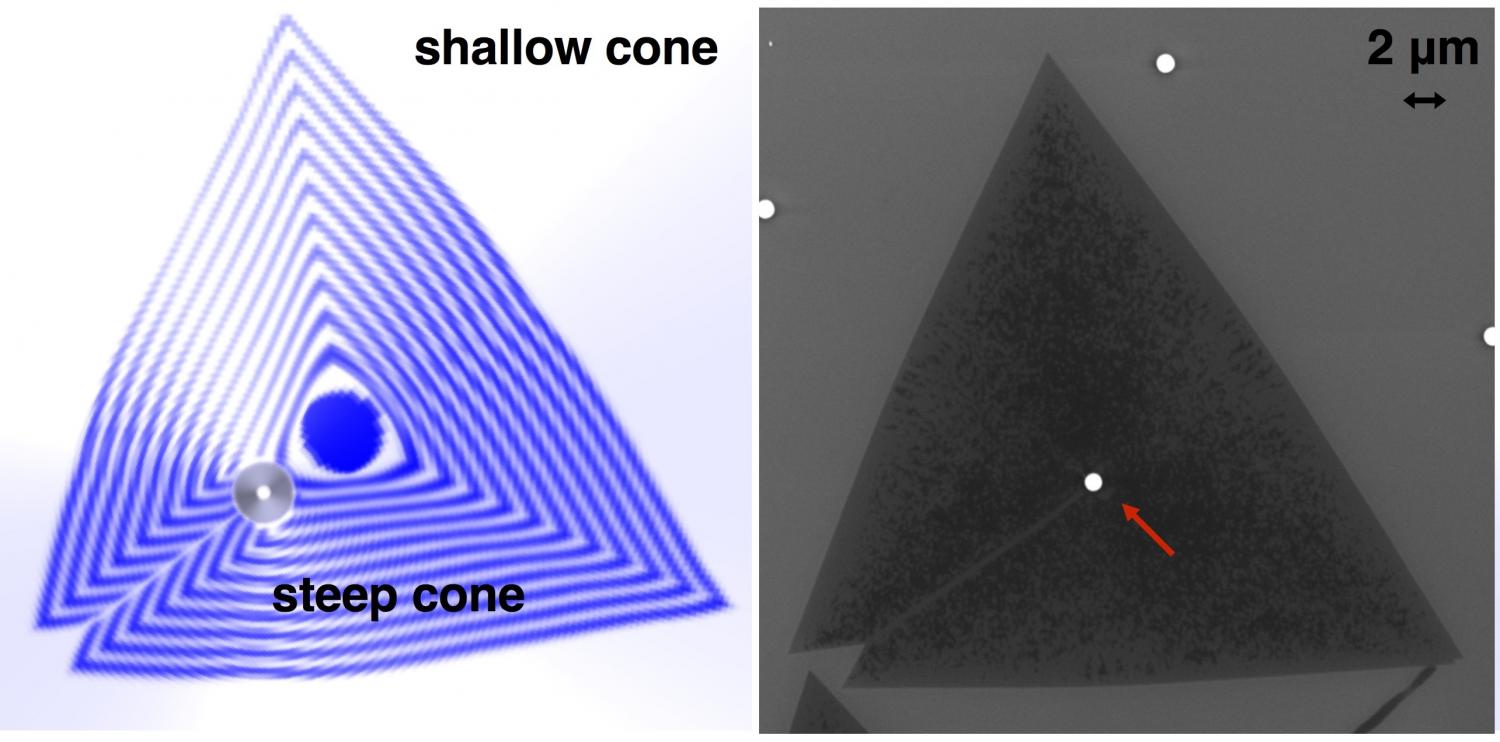
Researchers at Rice University and Oak Ridge National Laboratory predict and confirmed that two-dimensional materials grown onto a cone allows control over where defects called grain boundaries appear. At left, a Rice model predicts how a grain boundary would form on a steep cone and extend onto a shallow cone. Scientists at Oak Ridge confirmed the prediction when they created the material seen in an electron microscope image at right. (Credit: Rice University/Oak Ridge National Laboratory)
“The nonplanar shape of the substrate forces the 2-D crystal to grow in a curved ‘non-Euclidian’ space,” Yakobson said. “This strains the crystal, which occasionally yields by giving a way to the seams, or grain boundaries. It’s no different from the way a tailor would add a seam to a suit or a dress to fit a curvy customer.”
Modeling cones of different widths also revealed a “magic cone” of 38.9 degrees upon which growing a 2-D material would leave no grain boundary at all.
The Rice team extended its theory to see what would happen if the cones sat on a plane. They predicted how grain boundaries would form over the entire surface, and again, Oak Ridge experiments confirmed their results.
Yakobson said both the Rice and Oak Ridge teams were working on aspects of the research independently. “It was slow going until we met at a conference in Florida a couple of years back and realized that we should continue together,” he said. “It was certainly gratifying to see how experiments confirmed the models, while sometimes offering important surprises. Now we need to do the additional work to comprehend them as well.”