Research & Development World

  • R&D World Home
  • Topics
    • Aerospace
    • Automotive
    • Biotech
    • Careers
    • Chemistry
    • Environment
    • Energy
    • Life Science
    • Material Science
    • R&D Management
    • Physics
  • Technology
    • 3D Printing
    • A.I./Robotics
    • Software
    • Battery Technology
    • Controlled Environments
      • Cleanrooms
      • Graphene
      • Lasers
      • Regulations/Standards
      • Sensors
    • Imaging
    • Nanotechnology
    • Scientific Computing
      • Big Data
      • HPC/Supercomputing
      • Informatics
      • Security
    • Semiconductors
  • R&D Market Pulse
  • R&D 100
    • 2025 R&D 100 Award Winners
    • 2025 Professional Award Winners
    • 2025 Special Recognition Winners
    • R&D 100 Awards Event
    • R&D 100 Submissions
    • Winner Archive
  • Resources
    • Research Reports
    • Digital Issues
    • Educational Assets
    • R&D Index
    • Subscribe
    • Video
    • Webinars
    • Content submission guidelines for R&D World
  • Global Funding Forecast
  • Top Labs
  • Advertise
  • SUBSCRIBE

Semiconductor Nanowires Advance Flexible Photovoltaics

By AMOLF | May 29, 2019

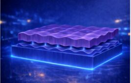
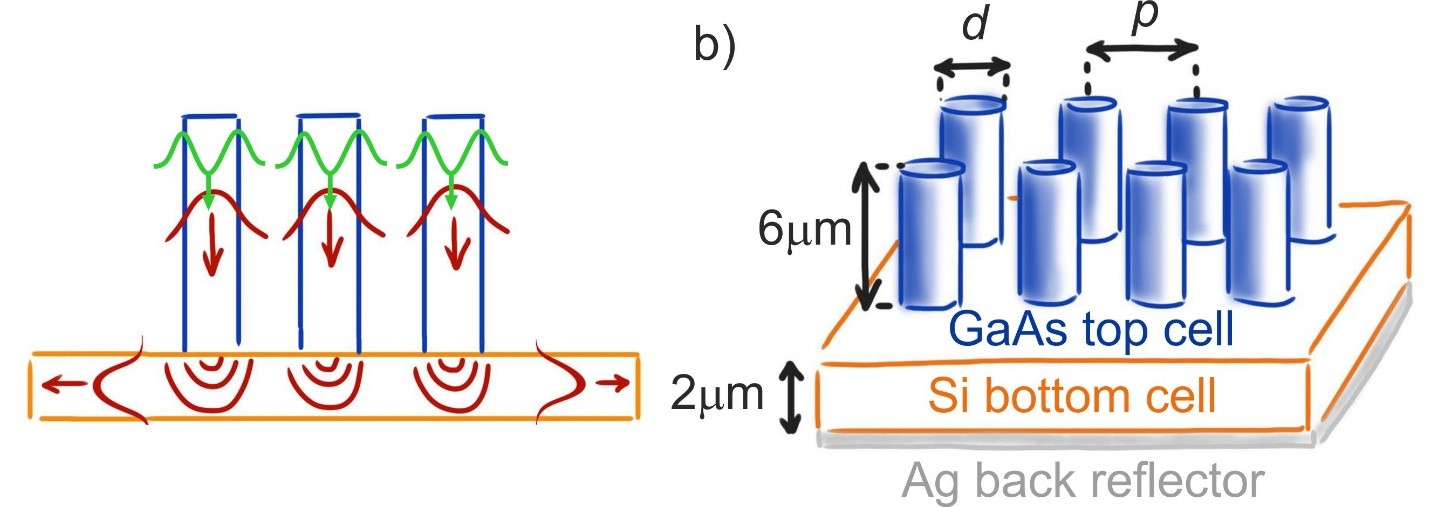
Optically coupled tandem of GaAs nanowires (6um tall) on silicon ultrathin film (2um). Sunlight is efficiently absorbed in each nanowire, and the array will transmit infrared light to be trapped into silicon film.

Capturing and manipulating light at nanoscale is a key factor to build high efficiency solar cells. Researchers in the 3D Photovoltaics group have recently presented a promising new design. Their simulations show that vertically stacked nanowires on top of ultrathin silicon films reduces the total amount of material needed by 90 percent while increasing the efficiency of the solar cell.

These promising simulation results are an important step towards new generation solar cells that are used in myriad ways in our buildings and landscape.

The results were published on May 23 in Optics Express.

A fascinating strategy to reduce both cost and rigidity is to combine ultrathin silicon photovoltaic films with semiconductor nanowire solar cells. The mechanical flexibility and resilience of micrometer thin cells make them well suited to apply on curved surfaces.

The idea is to optically couple the two materials stacked on top of each other as a tandem cell: a Gallium Arsenide (GaAs) nanowire array on top of an ultrathin silicon (2um-thick) film. GaAs vertical nanowires are well-known semiconductor components in photovoltaic applications.

Earlier experimental research in the 3D photovoltaics group has shown that such nanowires are able to absorb light ten to hundred times their geometrical cross section. Silicon, the second material in the tandem cell, is a highly desirable component thanks to the mature understanding of its optical and electronic properties as well as its widely available fabrication technologies.

The challenge researchers typically encounter when trying to downscale silicon to a few micrometers in thickness is that it compromises the solar cell’s performance due to poor absorption of infrared light. Light management strategies are therefore needed to compensate.

The research team decided to add vertically standing nanowires on top of silicon film and thereby make it up to four times more efficient in trapping infrared light in the silicon bottom cell.

Related Articles Read More >

Marktech expands large-area silicon photodiode portfolio for spectroscopy, medical diagnostics
R&D 100 Winner Spotlight: How Qnity beat the industry timeline on PFAS-free lithography
CEA-Leti achieves 400°C CMOS fabrication milestone for 3D chip stacking
Materials driving the next phase in semiconductor performance
rd newsletter
EXPAND YOUR KNOWLEDGE AND STAY CONNECTED
Get the latest info on technologies, trends, and strategies in Research & Development.
RD 25 Power Index

R&D World Digital Issues

Fall 2025 issue

Browse the most current issue of R&D World and back issues in an easy to use high quality format. Clip, share and download with the leading R&D magazine today.

R&D 100 Awards
Research & Development World
  • Subscribe to R&D World Magazine
  • Sign up for R&D World’s newsletter
  • Contact Us
  • About Us
  • Drug Discovery & Development
  • Pharmaceutical Processing
  • Global Funding Forecast

Copyright © 2026 WTWH Media LLC. All Rights Reserved. The material on this site may not be reproduced, distributed, transmitted, cached or otherwise used, except with the prior written permission of WTWH Media
Privacy Policy | Advertising | About Us

Search R&D World

  • R&D World Home
  • Topics
    • Aerospace
    • Automotive
    • Biotech
    • Careers
    • Chemistry
    • Environment
    • Energy
    • Life Science
    • Material Science
    • R&D Management
    • Physics
  • Technology
    • 3D Printing
    • A.I./Robotics
    • Software
    • Battery Technology
    • Controlled Environments
      • Cleanrooms
      • Graphene
      • Lasers
      • Regulations/Standards
      • Sensors
    • Imaging
    • Nanotechnology
    • Scientific Computing
      • Big Data
      • HPC/Supercomputing
      • Informatics
      • Security
    • Semiconductors
  • R&D Market Pulse
  • R&D 100
    • 2025 R&D 100 Award Winners
    • 2025 Professional Award Winners
    • 2025 Special Recognition Winners
    • R&D 100 Awards Event
    • R&D 100 Submissions
    • Winner Archive
  • Resources
    • Research Reports
    • Digital Issues
    • Educational Assets
    • R&D Index
    • Subscribe
    • Video
    • Webinars
    • Content submission guidelines for R&D World
  • Global Funding Forecast
  • Top Labs
  • Advertise
  • SUBSCRIBE