Researchers are applying the same “hydrodynamic transport model” used to study flow in fluids to explain heat transport in a solid semiconductor, with potential implications for the design of high-speed transistors and lasers.
Thermal imaging of tiny nanoscale semiconductor heat sources revealed details about vortices of heat-carrying objects called phonons.
The new findings have potentially important implications for “thermal crosstalk,” in which multiple heat sources next to each other impact the overall temperature of the system, hindering performance. The researchers used a technique called full-field thermoreflectance thermal imaging to directly visualize temperature changes produced by ultra-small heat sources, gold strips formed on top of the semiconductor indium gallium arsenide.
The research concerns the crucial role of phonons, quantum-mechanical objects, or “quasiparticles,” that describe how vibrations travel through a material’s crystal structure. The phonons are said to be “heat carriers” in solid materials.
“This is the first time such hydrodynamic effects are indirectly observed for heat propagation in a solid,” says Ali Shakouri, Purdue University’s Mary Jo and Robert L. Kirk Director of the Birck Nanotechnology Center and a professor of electrical and computer engineering. “While structures called vortices are common in fluid flows such as water or air, this is the first time we’ve seen that they can be present inside solids for phonon flow in the typical semiconductor indium gallium arsenide, which is used in high-speed transistors and lasers.”
Findings are detailed in a research paper published on Jan. 17 in Nature Communications.
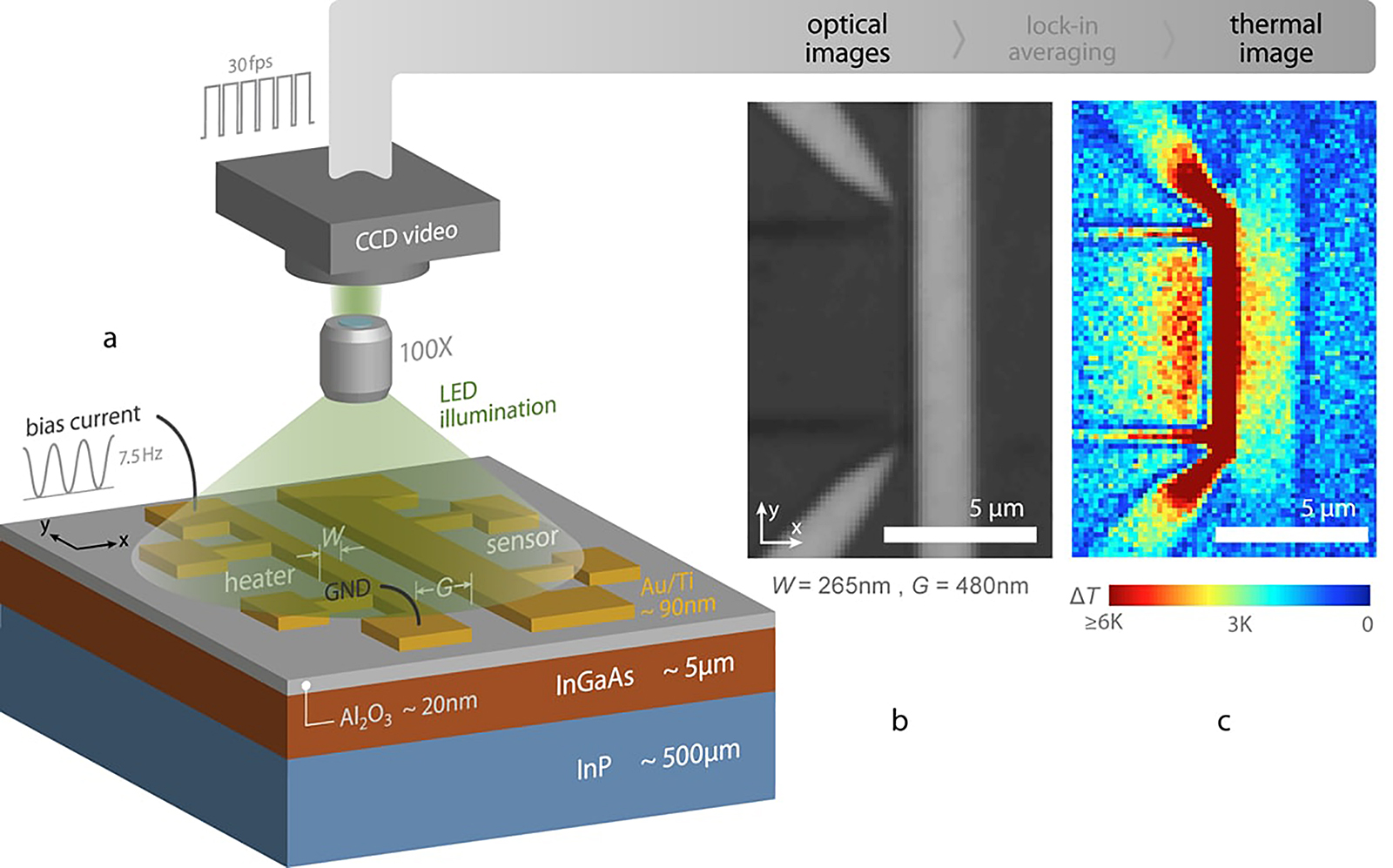
Purdue University researchers have visualized temperature changes produced by ultra-small heat sources, gold strips formed on top of the semiconductor indium gallium arsenide. The work has potential implications for the design of high-speed transistors and lasers. This image (a) depicts the device structure and experimental setup, an optical image (b) of the fabricated device and (c) an experimental thermal image. Image: Purdue University image/Amirkoushyar Ziabari, Bjorn Vermeersch
“The observed thermal crosstalk reduction has important implications in the design of nanoscale electronic and optoelectronic devices,” says Purdue postdoctoral research associate Amirkoushyar Ziabari, the paper’s lead author. “As the size of electronic and optoelectronic devices are getting smaller, there are more and more devices being packed into a smaller area, so the thermal crosstalk between these devices becomes important. Knowing the accurate thermal behavior in the neighborhood and a few microns from heat sources would help design better state-of-the-art devices in terms of performance, speed, thermal reliability, and so on.”
The researchers found that the reduced thermal crosstalk is caused by vortices generated near the edge of the heat sources.
“This is similar to the vortices that are observed at the edge of an obstacle placed inside of a current of air or water, such as behind an airplane wing,” Shakouri says.
The governing law of heat conduction, known as the Fourier Law or the heat-diffusion equation, does not accurately predict thermal transport for devices on the nanoscale. Because the Fourier diffusion equation doesn’t explain the heat transport at those scales, this transport regime is called non-diffusive.
“As the size of electronic and optoelectronic devices are getting smaller, it is important to consider this non-diffusive behavior for design and optimization of such small devices,” Ziabari says. “These new measurements show that at nanoscales, heat propagation has interesting ‘fluid-like’ behavior.”
Conventional methods do not account for vortices of heat transport found at the nanoscale.
“Vorticity only becomes important when the characteristic source dimension is comparable to the hydrodynamic length scale of about 150 nanometers,” he says.
The Fourier theory substantially overestimates the experimentally observed temperature a short distance away from the heater lines.
“The surprising effect was that the temperature decays much faster than what Fourier theory predicted,” Shakouri says. “Within a distance of 1 or 2 microns of a small heat source — a line about 100 nanometers wide – temperature could be one-third to one-fourth what Fourier theory predicts.”
The thermoreflectance thermal imaging approach allows researchers to create maps of temperature rise at far higher resolution than otherwise possible using light in the visible range.
The work was performed by researchers at the Birck Nanotechnology Center in Purdue’s Discovery Park, Purdue’s School of Electrical and Computer Engineering, Universitat Autónoma de Barcelona, Commissariat à l’Énergie Atomique in Grenoble, France, and the Department of Mechanical and Materials Engineering at the University of Cincinnati. All co-authors are listed in the abstract.
The research was partially funded by the European Commission and the Spanish Ministry of Economy and Competitiveness.
Source: Purdue University