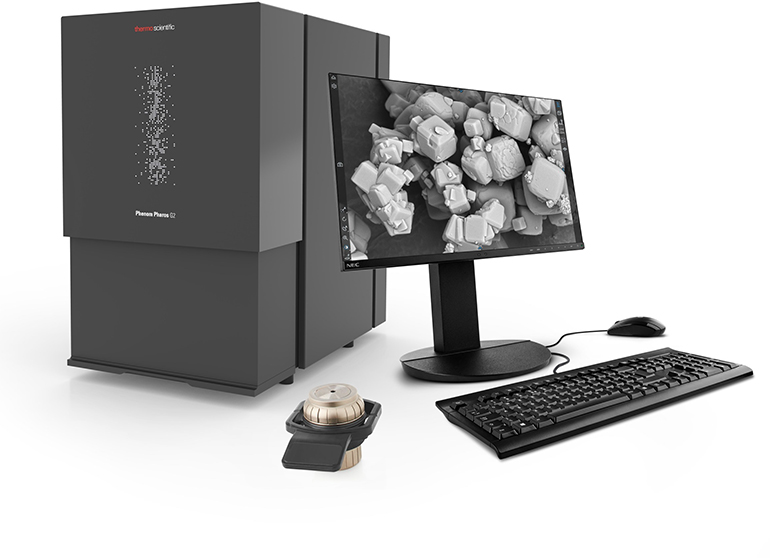
Thermo Scientific Phenom Pharos G2 Desktop Field Emission Gun – Scanning Electron Microscope (FEG-SEM)
Thermo Fisher Scientific announces the Thermo Scientific Phenom Pharos G2 Desktop Field Emission Gun – Scanning Electron Microscope (FEG-SEM) designed to increase access to advanced nanomaterial research capabilities. The new instrument makes it possible for customers to use a tabletop microscope to intuitively characterize the size, shape and chemical composition of a wide range of nanoparticles at high resolution.
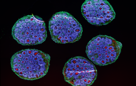
Using the Phenom Pharos G2, materials scientists can resolve the morphology of nanomaterials in materials like metals, minerals and ceramics at 2.0 nanometer (nm) resolution at 20 kilovolts (kV), paving the way to achieve advances in manufacturing, electronics, clean energy and other applications. Researchers can also image soft, beam-sensitive or insulating samples at energy levels as low as 1 kV, obtaining high-resolution views into polymers and multilayer organic films without damaging or obscuring their nanoscale features.
“The Phenom Pharos G2 progresses nanomaterial research by delivering high resolutions and a wide acceleration voltage range, all in a desktop system that can fit within a lab or office,” said Rosy Lee, VP and general manager of materials science at Thermo Fisher. “From more advanced textiles and food packaging to improved solar and wind energy, this easy-to-use instrument supports rapid innovation for a wide range of industries.”
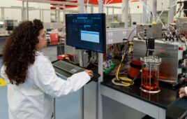
The Phenom Pharos G2 is intuitive to operate and highly productive, making it a versatile instrument for high-volume industrial and academic labs. The benefits include:
- High-resolution imaging: Users can obtain high-resolution images of 2.0 nm, compared to 2.5 nm with the previous version.
- Expanded energy range compared with the previous model: A wider acceleration voltage range of 1-20 kV provides versatility to image a wide range of samples.
- Fast time-to-image: Images can be obtained in just 30 seconds for high sample throughput.
- Ease-of-use: An intuitive user interface on a widescreen, 24-inch monitor with presets to simplify use and reduce human error when organizing workflows.
- Quick installation: Installation is 40% faster than the previous version, speeding time to results.
- Enhanced reliability: An integrated power supply and robust parts are designed to ensure the reproducibility of data and reduce interruptions to productivity.
To learn more about the Thermo Scientific Phenom Pharos G2 FEG-SEM, click here.