In case you missed it (ICYMI), here are some of the stories that made headlines in the world of cleanrooms and nanotechnology in the past week:
 Universities and research institutes in Britain have developed a system that can trap microbubbles, which allows scientists to study the bubbles’ properties and develop safer, more effective medical products. Microbubbles (gas bubbles that are smaller than 1 mm in size) are used in techniques that diagnose heart diseases and certain kinds of cancer. The addition of specific molecules to the shell of these bubbles could make them ideal vehicles for targeted medicine delivery and microsurgery.
 MIT scientists have created the first chip-fabrication technique that allows for significantly different materials to be deposited in the same layer. They’ve also developed chips with working versions of all the circuit components necessary to produce a general-purpose computer. To assemble their laterally integrated circuits, the researchers first deposit a layer of graphene on a silicon substrate. Then they etch it away in the regions where they wish to deposit the molybdenum disulfide. Next, at one end of the substrate, they place a solid bar of a material known as PTAS. They heat the PTAS and flow a gas across it and across the substrate. The gas carries PTAS molecules with it, and they stick to the exposed silicon but not to the graphene. Wherever the PTAS molecules stick, they catalyze a reaction with another gas that causes a layer of molybdenum disulfide to form. In previous work, the researchers characterized a range of materials that promote the formation of crystals of other compounds, any of which could be plugged into the process.
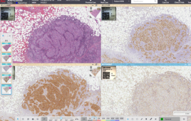
![Experimentally obtained image of a Fresnel zone plate (left) for focusing light that is fabricated with plasmon-assisted etching. A two-dimensional array of pillar-supported bowtie nanoantennas [zoomed in image (right)] comprises this flat lens.](/sites/cemag.us/files/University%20of%20Illinois.jpg) Finally, researchers in Illinois have come up with a simplified approach to fabricating flat, ultrathin optics. This technique enables simple etching without having to use acids or hazardous chemical etching agents. Laser light scans the template — a 2D array of gold pillar-supported bowtie nanoantennas (with an area of 80 x 80 square micrometers) — which is submerged in water, in a desired pattern in a microscope. The light-matter interaction, enhanced by the nanoantennas, produces a strong heating effect. As a result, the gold layer of the nanoantennas undergoes thermal expansion that works against its adhesion with their glass substrate. With certain amount of optical power, the force provided by thermal expansion allows the gold layer to break away from the substrate, etching the metal.
Finally, researchers in Illinois have come up with a simplified approach to fabricating flat, ultrathin optics. This technique enables simple etching without having to use acids or hazardous chemical etching agents. Laser light scans the template — a 2D array of gold pillar-supported bowtie nanoantennas (with an area of 80 x 80 square micrometers) — which is submerged in water, in a desired pattern in a microscope. The light-matter interaction, enhanced by the nanoantennas, produces a strong heating effect. As a result, the gold layer of the nanoantennas undergoes thermal expansion that works against its adhesion with their glass substrate. With certain amount of optical power, the force provided by thermal expansion allows the gold layer to break away from the substrate, etching the metal.