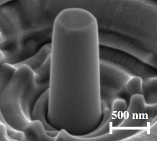
A scanning electron microscope image of one of the copper pillars used in the experiment. Credit: California Institute of Technology
Nanoscale deformations could impact the high-precision experiments, such as the Advanced Laser Interferometer Gravitational-Wave Observatory (LIGO)
A Caltech graduate student has shown that materials can undergo inelastic deformation prior to yielding, which could impact the design of materials, leading to stronger and tougher structures.
Xiaouye Ni, who studies materials science in the lab of Julia R. Greer, a Caltech professor of materials science and mechanics, has shown that metals undergo permanent deformation even prior to yielding—the threshold at which a material under strain becomes permanently deformed.
For example, take a metal ruler and bend it just a little bit. When you let go, it will spring right back to its original shape. But if you take that same ruler and bend it as hard as you can, it will reach a point known as the yield point where it stays permanently bent.
In materials science, the yielding phenomenon is explained as follows:
When you deform a material below its yield point, you’re just temporarily stretching the bonds between its atoms. There’s no permanent change happening to the material’s atomic-level structure and the deformation is completely recoverable and instantaneous. This temporary stretching is called elastic deformation.
Deform a metal past its yield point and you cause the movement of preexisting line defects known as dislocations, which contribute to the permanent deformation. The dislocations move through the crystal lattice, creating more dislocations as they go and tangling up on each other. The motion of these disclocation results in permanent plastic deformation.
The yield point is usually considered to be a discrete phenomenon—that is, dislocations start moving when a material is strained beyond its yield point. However, Ni’s data show that there are at an atomic level, irreversible changes in the structure of a material as soon as a material begins to deform, long before it reaches its yield point.
“Every materials scientist and every textbook in the world will tell you that when you deform any material—it can be a metal, wood, any kind of textile, anything—the first thing that occurs is elastic deformation that will instantly recover,” Greer says. “It is the most fundamental belief that just about every mechanical and materials science course relies on.”
To explore what was happening in a material under strain, Xiaouye fabricated copper pillars that are 500 nanometers wide (a human hair is 200 times thicker) and pressed on them with a diamond stylus.
The stylus applied fixed amounts of pressure less than the copper’s yield point and then oscillated up and down slightly.
What she found was that after being subjected to those oscillations, the pillars were slow to return to their original, undeformed shape.
“If the deformation were purely elastic, that wouldn’t happen because it would recover instantaneously,” Xiaouye says.
The sluggish reaction showed that the pillars had developed an internal resistance, a hallmark of inelastic deformation.
“What Xiaouye’s data are showing is that from the first moment you start deforming it, the dislocations start being active,” Greer says. Now that we know how to do this, we can probe a variety of different classes of materials.
Xiaouye says the discovery is likely to find applications in many fields of study.”You can actually use this signature to see how close you are to the catastrophic failure point,” Xiaouye says. Also, for high-precision experiments, as the Advanced Laser Interferometer Gravitational-Wave Observatory (LIGO)—which detected gravitational waves for the first time in 2016—even nanoscale dislocations can create a noise that it is imperative to understand and remove.
The study, “Probing Microplasticity in Small-Scale FCC Crystals via Dynamic Mechanical Analysis,” appeared in the April 14 issue of Physical Review Letters.