Research & Development World

  • R&D World Home
  • Topics
    • Aerospace
    • Automotive
    • Biotech
    • Careers
    • Chemistry
    • Environment
    • Energy
    • Life Science
    • Material Science
    • R&D Management
    • Physics
  • Technology
    • 3D Printing
    • A.I./Robotics
    • Software
    • Battery Technology
    • Controlled Environments
      • Cleanrooms
      • Graphene
      • Lasers
      • Regulations/Standards
      • Sensors
    • Imaging
    • Nanotechnology
    • Scientific Computing
      • Big Data
      • HPC/Supercomputing
      • Informatics
      • Security
    • Semiconductors
  • R&D Market Pulse
  • R&D 100
    • 2025 R&D 100 Award Winners
    • 2025 Professional Award Winners
    • 2025 Special Recognition Winners
    • R&D 100 Awards Event
    • R&D 100 Submissions
    • Winner Archive
  • Resources
    • Research Reports
    • Digital Issues
    • Educational Assets
    • R&D Index
    • Subscribe
    • Video
    • Webinars
    • Content submission guidelines for R&D World
  • Global Funding Forecast
  • Top Labs
  • Advertise
  • SUBSCRIBE

Water makes wires even more nano

By R&D Editors | April 6, 2015

These nanowires were created at Rice Univ. through a process called meniscus-mask lithography. From left, they’re made of silicon, silicon dioxide, gold, chromium, tungsten, titanium, titanium dioxide and aluminum. The scale bar is 1 micron for all images. Image: Tour Group/Rice Univ.Water is the key component in a Rice Univ. process to reliably create patterns of metallic and semiconducting wires less than 10 nm wide.

The technique by the Rice lab of chemist James Tour builds upon its discovery that the meniscus—the curvy surface of water at its edge—can be an effective mask to make nanowires.

The Rice team of Tour and graduate students Vera Abramova and Alexander Slesarev have now made nanowires between 6 and 16 nm wide from silicon, silicon dioxide, gold, chromium, tungsten, titanium, titanium dioxide and aluminum. They have also made crossbar structures of conducting nanowires from one or more of the materials.

A paper on their technique, called meniscus-mask lithography, has been published online by Nano Letters.

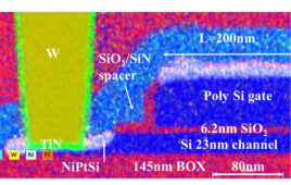
The process is promising for the semiconductor industry as it seeks to make circuits ever smaller. State-of-the-art integrated circuit fabrication allows for signal wires that approach 10 nm, visible only with powerful microscopes. These are the paths that connect the billions of transistors in modern electronic devices.

“This could have huge ramifications for chip production since the wires are easily made to sub-10-nm sizes,” Tour said of the Rice process. “There’s no other way in the world to do this en masse on a surface.”

Current approaches to making such tiny wires take several paths. Lithography, the standard method for etching integrated circuits, is approaching the physical limits of its ability to shrink them further. Bulk synthesis of semiconducting and metallic nanowires is also possible, but the wires are difficult to position in integrated circuits.

Water’s tendency to adhere to surfaces went from an annoyance to an advantage when the Rice researchers found they could use it as a mask to make patterns. The water molecules gather wherever a raised pattern joins the target material and forms a curved meniscus created by the surface tension of water.

The meniscus-mask process involves adding and then removing materials in a sequence that ultimately leaves a meniscus covering the wire and climbing the sidewall of a sacrificial metal mask that, when etched away, leaves the nanowire standing alone.

Tour said the process should work with modern fabrication technology with no modifications to existing equipment and minimal changes in fabrication protocols. No new tools or materials are needed.

Source: Rice Univ.

ENTRIES OPEN:
Establish your company as a technology leader. For 50 years, the R&D 100 Awards, widely recognized as the “Oscars of Invention,” have showcased products of technological significance. Learn more.

Related Articles Read More >

R&D 100 winner LLNL achieves 1,000x speed boost in 3D nanofabrication
CEA-Leti achieves 400°C CMOS fabrication milestone for 3D chip stacking
The 2025 R&D 100 Finalists are here
New nanotechnology method increases microalgae biofuel yield by 300%
rd newsletter
EXPAND YOUR KNOWLEDGE AND STAY CONNECTED
Get the latest info on technologies, trends, and strategies in Research & Development.
RD 25 Power Index

R&D World Digital Issues

Fall 2025 issue

Browse the most current issue of R&D World and back issues in an easy to use high quality format. Clip, share and download with the leading R&D magazine today.

R&D 100 Awards
Research & Development World
  • Subscribe to R&D World Magazine
  • Sign up for R&D World’s newsletter
  • Contact Us
  • About Us
  • Drug Discovery & Development
  • Pharmaceutical Processing
  • Global Funding Forecast

Copyright © 2025 WTWH Media LLC. All Rights Reserved. The material on this site may not be reproduced, distributed, transmitted, cached or otherwise used, except with the prior written permission of WTWH Media
Privacy Policy | Advertising | About Us

Search R&D World

  • R&D World Home
  • Topics
    • Aerospace
    • Automotive
    • Biotech
    • Careers
    • Chemistry
    • Environment
    • Energy
    • Life Science
    • Material Science
    • R&D Management
    • Physics
  • Technology
    • 3D Printing
    • A.I./Robotics
    • Software
    • Battery Technology
    • Controlled Environments
      • Cleanrooms
      • Graphene
      • Lasers
      • Regulations/Standards
      • Sensors
    • Imaging
    • Nanotechnology
    • Scientific Computing
      • Big Data
      • HPC/Supercomputing
      • Informatics
      • Security
    • Semiconductors
  • R&D Market Pulse
  • R&D 100
    • 2025 R&D 100 Award Winners
    • 2025 Professional Award Winners
    • 2025 Special Recognition Winners
    • R&D 100 Awards Event
    • R&D 100 Submissions
    • Winner Archive
  • Resources
    • Research Reports
    • Digital Issues
    • Educational Assets
    • R&D Index
    • Subscribe
    • Video
    • Webinars
    • Content submission guidelines for R&D World
  • Global Funding Forecast
  • Top Labs
  • Advertise
  • SUBSCRIBE