By Brian W. Anthony
Close-up view on a colorful nanotechnology electronic system 3D rendering
Nanotechnology continues to make headlines as use cases increase across a variety of industry sectors, ranging from medicine and homeland security to transportation, food and retail. But when it comes right down to it, the nanoscale is nothing more than a dimension; it’s just really, really small. Is it the size alone that is so captivating or are there other reasons nanoscience repeatedly garners so much attention?
Here’s what you need to know about this rapidly evolving and revolutionary landscape:
The nanoscale is unique
One nanometer is a billionth of a meter, or 10-9 of a meter. Not only is that extremely small, it also happens to be the scale at which biology — meaning life itself — occurs. In addition, the nanoscale is the realm where quantum effects start to come into play. As a result, any knowledge or intuition you have about physical systems and how they behave may not apply when working at the nanoscale. Consider graphite, a form of carbon familiar to us as the lead in a No. 2 pencil. A decade ago researchers figured out how to create sheets of graphite just one atom thick. This is graphene, the thinnest material known to exist. Flexible, lightweight, and incredibly conductive electrically, it’s also the strongest material known to humanity — 200 times stronger than steel.
Fabrication or manufacturing and characterizing at the nanoscale require specialized capabilities
When you’re working at the nanoscale, you have to control environmental conditions such as temperature, humidity, air quality, and electromagnetic interference down to the sub-nanometer level. Why? Because impurities as small as a speck of dust, a skin cell, or even a single, subtle vibration are generally much larger than a nanometer, and if you’re trying to either build or characterize at this scale, any contaminants like these will impede you.
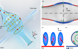
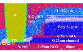
In addition to needing a particle and interference-free environment, manufacturers working at the nanoscale need to expand their toolboxes. Some need highly specialized equipment because they are fabricating novel materials, such as very thin membranes that are submicron and down to a single atom thick. These membranes can be used as high-temperature semiconductors, or they can produce optical fields that are useful for computation and machine learning. Likewise, those working to characterize at the nanoscale also require sophisticated tools, like a cryo-electron microscope, which can pass electron beams through material samples from different orientations. It’s analogous in some ways to a CT imager, a computed tomography imager that is used for medical imaging, but it works at the subcellular level.
Nanotechnology use cases are broad
Researchers across all scientific disciplines — materials, photovoltaics, computation, chemistry and biologics, to name just a few — are developing applications for nanotechnology. Here’s a particularly relevant example: Let’s say you want to characterize the aerosol patterns in exhaled breath. To do so, you need to determine not only the particle count, but also the mix of solid particles and fluid particles, their chemical constituents, and the particle sizes. This could all be possible using a combination of photonics at the nanoscale to characterize air-suspended fluids and air-suspended particulates in a breath.
Data drives the processes, and the processes generate massive amounts of data
Working at the nanoscale involves enormous amounts of data. You rely on it for establishing the right conditions and for operating your equipment. Then, once you begin imaging something or, say, defining spatially distributed measurements of a surface at the nanoscale, you start generating even bigger data sets. Nanoscience wouldn’t be possible without massive quantities of data, both as inputs and outputs. In order to connect the physical to the digital for nano applications, it is critical to be able to understand, manage, process, and utilize these data streams.
Nanotechnology offers vast opportunities for innovation. With improved understanding and greater accessibility of toolsets for the fabrication, study, and manipulation of nanoscale structures and systems, we will continue to move forward with this revolutionary way of understanding and working with matter.
About Brian W. Anthony
Professor Anthony is the co-director of MIT’s Medical Electronic Device Realization Center and associate director of MIT.nano. He is also a lead instructor of the 3-day MIT Professional Education course, Nanoscience and Nanotech: Industrial Application and Transformation, which takes place July 13-15, 2020. With more than 25 years of experience in product realization, Dr. Anthony designs instruments and techniques to monitor and control physical systems. His work involves systems analysis and design, calling upon mechanical, electrical, and optical engineering, along with computer science and optimization.