Research & Development World

  • R&D World Home
  • Topics
    • Aerospace
    • Automotive
    • Biotech
    • Careers
    • Chemistry
    • Environment
    • Energy
    • Life Science
    • Material Science
    • R&D Management
    • Physics
  • Technology
    • 3D Printing
    • A.I./Robotics
    • Software
    • Battery Technology
    • Controlled Environments
      • Cleanrooms
      • Graphene
      • Lasers
      • Regulations/Standards
      • Sensors
    • Imaging
    • Nanotechnology
    • Scientific Computing
      • Big Data
      • HPC/Supercomputing
      • Informatics
      • Security
    • Semiconductors
  • R&D Market Pulse
  • R&D 100
    • Call for Nominations: The 2025 R&D 100 Awards
    • R&D 100 Awards Event
    • R&D 100 Submissions
    • Winner Archive
    • Explore the 2024 R&D 100 award winners and finalists
  • Resources
    • Research Reports
    • Digital Issues
    • R&D Index
    • Subscribe
    • Video
    • Webinars
  • Global Funding Forecast
  • Top Labs
  • Advertise
  • SUBSCRIBE

How chiral asymmetry could pave the way for high-efficiency electronics

By R&D Editors | September 3, 2024

Researchers at the U.S. Department of Energy have announced the manipulation of quantum properties of graphene, the single-atom-thick layer of carbon that has captivated researchers for about two decades.

In their research, scientists constructed quantum electronic devices using a bespoke configuration of graphene layers: a twisted monolayer–bilayer graphene structure. This setup consists of a single layer of graphene placed on top of two layers of graphene (bilayer), with a slight rotational misalignment. This created what is known as a moiré superlattice, which exhibits chiral edge states — one-way paths for electrons along the edges of the material.

Scanning tunneling microscope map of a device made of three atomic layers of graphene

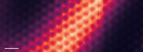
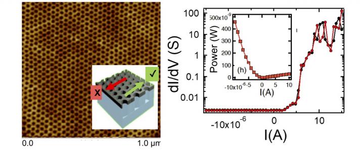
Scanning tunneling microscope map of a device made of three atomic layers of graphene, showing the wave function of a chiral interface state (bright stripe) between two insulating regions with opposite chirality (dark sides). [Credit: Lawrence Berkeley National Laboratory]

Tuning electron density

By tuning electron density with a gate electrode, the scientists created neighboring regions with opposing topological properties, enabling the control of the direction of electron flow. The unique properties of these chiral interface also suppress electron collisions, potentially supporting near-zero resistance electron transport.

Using a scanning tunneling microscope, researchers could visualize these chiral states with atomic resolution, move them like pieces on a quantum chessboard. They could also even ‘write’ or ‘delete’ them at will. This allowed them to characterize the channels’ properties and spatial distribution. This research contributes significantly to our understanding of topological phenomena in two-dimensional materials, a field that explores how the “shape” or topology of a material can influence its electronic properties.

The research was the subject of a paper from Zhang et al. published in Nature Physics.

How it works in a nutshell

In their research, the scientists created a moiré system using twisted monolayer–bilayer graphene, which hosts correlated and topological states that support electrical controlled via applied gate voltages. .

By tuning the carrier concentration, the team stabilized neighboring domains with opposite Chern numbers. This created topological interfaces without any structural boundaries, allowing for direct imaging of the chiral interface states using a scanning tunneling microscope.

As the research Nature Physics abstract explained:

Moiré systems made from stacked two-dimensional materials host correlated and topological states that can be electrically controlled with applied gate voltages. One prevalent form of topological state that can occur are Chern insulators that display a quantum anomalous Hall effect. Here we manipulate Chern domains in an interaction-driven quantum anomalous Hall insulator made from twisted monolayer–bilayer graphene and observe chiral interface states at the boundary between different domains. By tuning the carrier concentration, we stabilize neighbouring domains of opposite Chern number that then provide topological interfaces devoid of any structural boundaries. This allows the wavefunction of chiral interface states to be directly imaged using a scanning tunnelling microscope. Our theoretical analysis confirms the chiral nature of observed interface states and allows us to determine the characteristic length scale of valley polarization reversal across neighbouring Chern domains.

The Department of Energy Office of Science, the National Science Foundation, and various international organizations and foundations backed the research.

Related articles from the R&D World archives

Light Induces Magnetization in Certain Semiconductors

Light Induces Magnetization in Certain Semiconductors

University of Waterloo chemists reported finding in 2018 a much faster and more efficient way to store and process information by expanding the limitations of how the flow of electricity can be used and managed.

Read More

New Semiconductor Pushes Spintronics Toward Reality

New Semiconductor Pushes “Spintronics” Toward Reality

Created from an entirely new “low symmetry” crystal structure, the compound is the first to build spintronic properties into a material that’s stable at room temperature and easily tailored to a variety of applications.

Read More

New Device could Increase Battery Life of Electronics by a Hundred-Fold

New Device could Increase Battery Life of Electronics by a Hundred-Fold

Among the chief complaints for smartphone, laptop and other battery-operated electronics users is that the battery life is too short and–in some cases–that the devices generate heat. In 2018, a group of physicists led by Deepak K. Singh, associate professor of physics and astronomy at the University of Missouri, developed a device material that can address both issues.

Read More

Related Articles Read More >

First CRISPR-edited spider spins red fluorescent silk
KIST carbon nanotube supercapacitor holds capacity after 100,000 cycles
A new wave of metalworking lets semiconductor crystals bend and stretch
LLNL deposits quantum dots on corrugated IR chips in a single step
rd newsletter
EXPAND YOUR KNOWLEDGE AND STAY CONNECTED
Get the latest info on technologies, trends, and strategies in Research & Development.
RD 25 Power Index

R&D World Digital Issues

Fall 2024 issue

Browse the most current issue of R&D World and back issues in an easy to use high quality format. Clip, share and download with the leading R&D magazine today.

Research & Development World
  • Subscribe to R&D World Magazine
  • Enews Sign Up
  • Contact Us
  • About Us
  • Drug Discovery & Development
  • Pharmaceutical Processing
  • Global Funding Forecast

Copyright © 2025 WTWH Media LLC. All Rights Reserved. The material on this site may not be reproduced, distributed, transmitted, cached or otherwise used, except with the prior written permission of WTWH Media
Privacy Policy | Advertising | About Us

Search R&D World

  • R&D World Home
  • Topics
    • Aerospace
    • Automotive
    • Biotech
    • Careers
    • Chemistry
    • Environment
    • Energy
    • Life Science
    • Material Science
    • R&D Management
    • Physics
  • Technology
    • 3D Printing
    • A.I./Robotics
    • Software
    • Battery Technology
    • Controlled Environments
      • Cleanrooms
      • Graphene
      • Lasers
      • Regulations/Standards
      • Sensors
    • Imaging
    • Nanotechnology
    • Scientific Computing
      • Big Data
      • HPC/Supercomputing
      • Informatics
      • Security
    • Semiconductors
  • R&D Market Pulse
  • R&D 100
    • Call for Nominations: The 2025 R&D 100 Awards
    • R&D 100 Awards Event
    • R&D 100 Submissions
    • Winner Archive
    • Explore the 2024 R&D 100 award winners and finalists
  • Resources
    • Research Reports
    • Digital Issues
    • R&D Index
    • Subscribe
    • Video
    • Webinars
  • Global Funding Forecast
  • Top Labs
  • Advertise
  • SUBSCRIBE