Research & Development World

  • R&D World Home
  • Topics
    • Aerospace
    • Automotive
    • Biotech
    • Careers
    • Chemistry
    • Environment
    • Energy
    • Life Science
    • Material Science
    • R&D Management
    • Physics
  • Technology
    • 3D Printing
    • A.I./Robotics
    • Software
    • Battery Technology
    • Controlled Environments
      • Cleanrooms
      • Graphene
      • Lasers
      • Regulations/Standards
      • Sensors
    • Imaging
    • Nanotechnology
    • Scientific Computing
      • Big Data
      • HPC/Supercomputing
      • Informatics
      • Security
    • Semiconductors
  • R&D Market Pulse
  • R&D 100
    • 2025 R&D 100 Award Winners
    • 2025 Professional Award Winners
    • 2025 Special Recognition Winners
    • R&D 100 Awards Event
    • R&D 100 Submissions
    • Winner Archive
  • Resources
    • Research Reports
    • Digital Issues
    • Educational Assets
    • Subscribe
    • Video
    • Webinars
    • PharmSci360
    • Content submission guidelines for R&D World
  • Global Funding Forecast
  • Top Labs
  • Advertise
  • SUBSCRIBE

High-Energy Ions’ Movement Affected by Silicon Crystal Periodicity

By Springer | March 22, 2018

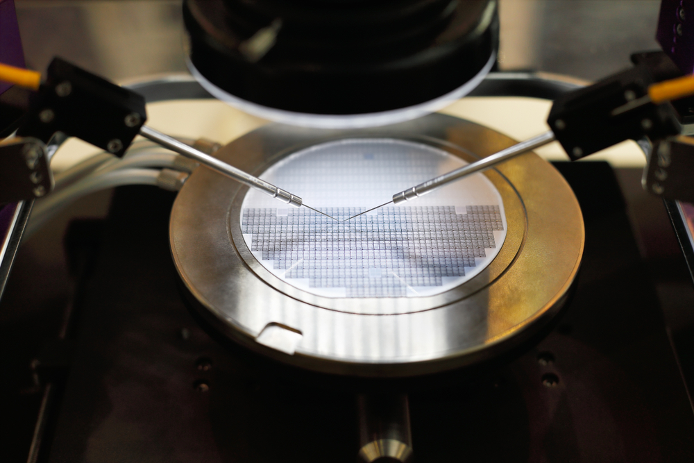
The thinner the silicon crystal, the better. Indeed, thinner crystals provide better ways to manipulate the trajectories of very high-energy ions in particle accelerators. Further applications include materials analysis, semiconductor doping and beam transport in large particle accelerators. All of these rely on our understanding of how positively-charged high-energy particles move through crystals. This process, called ion channelling, is the focus of a new paper by Mallikarjuna Motapothula and Mark Breese working at the National University of Singapore. In a paper published in EPJ B, the authors study how the crystal periodicity affects the motion of ions whose energy belongs to a 1 to 2 MeV range, as they are transmitted through very thin crystals on the order of a few hundred nanometres, and how it impacts their angular distribution.

Channelling in crystals occurs when the transverse energy of incident ions is less than the maximum potential energy associated with an atom row or a crystal plane. The authors study the trajectories of high-energy ions, which pass through several radial rings of atomic strings before exiting the thin crystal. Each ring may focus, steer or scatter the channelled ions in the transverse direction.

What is so interesting about this work is that it relies on an advanced process of fabricating much thinner crystals than was previously possible, reaching 55 nanometres. This, in turn, makes it possible to observe much more sensitive and fine angular structures in the distribution of transmitted ions.

Thanks to such advanced materials, the authors found that several previously observed but poorly understood phenomena related to ion channelling can now be explained. These phenomena are related to the fact that ions approach the crystal nuclei within a certain range of distances and are scattered through an angle large enough for them to interact with several adjacent atoms before exiting the thin crystal with a distinctive angular distribution.
Related Articles Read More >

Researchers develop sawdust-based foam as polystyrene bans force industry to adapt
Researchers develop compostable PLA that potentially could be used for biomedical applications
Elkem Silicones rebrands as Bluestar Silicones after ownership change
How Atomis is using AI simulations to commercialize MOFs
rd newsletter
EXPAND YOUR KNOWLEDGE AND STAY CONNECTED
Get the latest info on technologies, trends, and strategies in Research & Development.

R&D World Digital Issues

Fall 2025 issue

Browse the most current issue of R&D World and back issues in an easy to use high quality format. Clip, share and download with the leading R&D magazine today.

R&D 100 Awards
Research & Development World
  • Subscribe to R&D World Magazine
  • Sign up for R&D World’s newsletter
  • Contact Us
  • About Us
  • Drug Discovery & Development
  • Pharmaceutical Processing
  • Global Funding Forecast

Copyright © 2026 Arrowfly LLC. All Rights Reserved. The material on this site may not be reproduced, distributed, transmitted, cached or otherwise used, except with the prior written permission of Arrowfly
Privacy Policy | Advertising | About Us

Search R&D World

  • R&D World Home
  • Topics
    • Aerospace
    • Automotive
    • Biotech
    • Careers
    • Chemistry
    • Environment
    • Energy
    • Life Science
    • Material Science
    • R&D Management
    • Physics
  • Technology
    • 3D Printing
    • A.I./Robotics
    • Software
    • Battery Technology
    • Controlled Environments
      • Cleanrooms
      • Graphene
      • Lasers
      • Regulations/Standards
      • Sensors
    • Imaging
    • Nanotechnology
    • Scientific Computing
      • Big Data
      • HPC/Supercomputing
      • Informatics
      • Security
    • Semiconductors
  • R&D Market Pulse
  • R&D 100
    • 2025 R&D 100 Award Winners
    • 2025 Professional Award Winners
    • 2025 Special Recognition Winners
    • R&D 100 Awards Event
    • R&D 100 Submissions
    • Winner Archive
  • Resources
    • Research Reports
    • Digital Issues
    • Educational Assets
    • Subscribe
    • Video
    • Webinars
    • PharmSci360
    • Content submission guidelines for R&D World
  • Global Funding Forecast
  • Top Labs
  • Advertise
  • SUBSCRIBE