 Product developments, required to solve some of the most challenging societal issues, increasingly rely on materials scientists to provide innovation in new materials or combinations of existing materials to achieve desired performance. Characterizing and understanding the detailed structure of materials at the atomic level is essential to these initiatives, and cannot be achieved without advanced imaging and analytical techniques. Transmission electron microscopy (TEM), in particular, has been a key tool in advancing these insights.
In recent years, TEMs have provided materials scientists with some of the most powerful insights towards the ‘atomic engineering’ of improved material properties. One example is the improvement in the performance of certain types of steels to make them both stronger and lighter in transportation use cases to improve fuel efficiency without detriment to passenger safety in the event of accidents. Similar advances have enabled smarter product design and materials decisions across industries.
The evolution of electron microscopy and the importance of integrated (S)TEM
TEM technology has evolved significantly in recent years. From the ‘atomic imaging only’ tools of a few decades ago to sophisticated, highly integrated sub-atomic resolution analytical characterization tools of today. Now newer instruments known as (S)TEMs, where the ‘S’ refers to scanning, have the ability to form atomic level chemical maps in addition to images using electron probes that scan across samples and stimulate different types of chemical information from individual atomic columns in the sample. Coupling analytical detection capabilities such as electron energy loss spectroscopy (EELS) with the (S)TEM column has helped scientists better understand the fine details of the chemistry of materials. Today, technology providers making these advanced analytical (S)TEMs are working to achieve improved performance and deeper multimodal integration (between analytical detectors, imaging cameras and software acquisition) to provide higher quality data for a broader range of use cases and with lower thresholds for expertise.
This integration provides a seamless user experience bringing together these once ‘stand alone’ complex capabilities into one easy to use solution. Another key integrated chemical mode is the more classical energy dispersive spectroscopy (EDS), which detects X-Ray information as the probe scans across the sample. The addition of an integrated electrostatic beam blanker with imaging and chemical capabilities provides incredible flexibility in how high quality atomic level data can be captured from a broader range of materials, providing insights that were not possible to imagine previously.
With these fully integrated capabilities, materials scientists can better understand the relationships between structure, function, property and the chemistry of specific materials or combinations of materials. For example, atomic positioning can be directly observed with the (S)TEM, chemistry of atoms can be revealed by the combination of EDS and EELS, and with EELS further information on how atoms are bonded to each other can be found. Beam blanking then offers control of the way the structure is scanned to help provide information from electron beam sensitive materials. This deeper understanding makes it possible for scientists to not only more fully understand the makeup of certain materials, but also how materials work together and interact with the environments they end up in as part of end use products.
Advanced technologies enabling deeper insights
Without electron microscopes, the rapid growth and advancement of computing and mobile technology over the past three decades and more recently artificial intelligence could not have happened since the fundamental understanding of materials and product behavior required to improve semiconductor chip performance would not have been possible. The developers of the device technology simply cannot see what they have made without TEMs and so cannot understand why they fail or how performance could be improved. Modern integrated (S)TEMs are enabling the development of next generation devices and emerging solutions involving Quantum approaches. Other examples include scientific discoveries that are helping transform the way we live by providing a deeper understanding of materials in emerging industries such as sustainable solutions, as well as next generation batteries or catalysts used to clean our air or in the production of fertilizers.
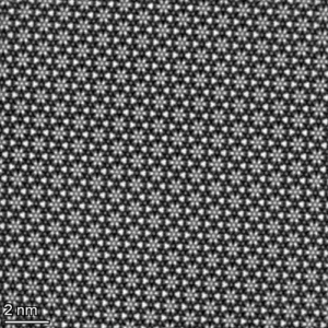
Another specific example is the area of research into 2D materials, such as graphene, molybdenum disulfide (MoS2) and hexagonal boron nitride (h-BN). This field has gained attention in recent years due to its applications in electronics, energy storage and more. With (S)TEMs, scientists have been able to precisely identify the atomic structures within 2D materials, as well as detect defects and other structural features necessary to develop and manufacture usable products.
Overcoming common challenges with (S)TEM
Integrated (S)TEM can help modern scientists overcome longstanding industry challenges. In addition to offering higher flexibility and unparalleled insights into complex materials systems, next-generation (S)TEMs help materials scientists easily quantify data with multimodalities as they look to engage in precise chemical and structural investigations of broad classes of modern materials – including those that were once impossible due to their sensitivity to electron beam damage.
This technology is also accessible to scientists of all skill levels, as it is easy to operate and allows them to focus on scientific discoveries versus lab operations. As opposed to previous generations, the latest (S)TEMs make it possible for materials scientists – rather than just expert electron microscopists – to gain more precise insights into complex investigations of difficult modern materials.
As scientists look to deploy the technology, lab managers can look to providers who specialize in seamlessly integrated atomic level analytical solutions. Although not required, choosing one supplier who can provide all the necessary hardware and software can support more streamlined workflows for the user with higher quality data to deliver otherwise unobtainable insights. Depending on the supplier, scientists can control the level of automation and personalization that comes with the technology to align with the lab’s specific use cases.
The industries where the (S)TEM is sparking growth
The (S)TEM can be utilized across industries, such as in battery research, catalysis and quantum computing. The battery industry is one industry where the application of the (S)TEM is growing rapidly, driven by the demand for EVs and energy storage. Scientists can use the technology as an effective characterization tool for battery materials and cell manufacturers during materials research and development (R&D), quality control and failure analysis. One specific example of how scientists are using the (S)TEM in battery R&D includes gaining more precise imaging of cathodes and anodes — two important components needed to construct a battery. In addition, advanced (S)TEM tools can provide key insights into how chemistries develop and change during battery charging and discharging cycles.
Beyond batteries, (S)TEMs are used in catalysis research to aid in understanding catalytic reactions. Other advanced techniques are important here such as 4D-STEM, atomic electron tomography, cryogenic electron microscopy, monochromated EELS and even in-situ environmental (gaseous) exposure and control. These techniques aim to enhance scientists’ knowledge of catalyst behavior, which ultimately helps them create higher quality, more efficient or more sustainable catalysts for pollution control (automotive or energy production) or fertilizer production.
Quantum computing is in development and the research into which materials will be best to enable productization is highly active. Quantum computing relies on materials that have limited defects. (S)TEMs help to identify and characterize these materials, their structures and defects to help determine the best choices to provide the best performance and the best chance of being used in manufacture of products in the future.
Reaching new discoveries with the (S)TEM
Today, integrated (S)TEMs are aiding some of the greatest scientific discoveries and breakthroughs in materials science due to the advanced imaging techniques that they enable, such as research into 2D materials, battery R&D, catalysis, next generation sensors and devices, quantum computing, advanced steels and other metal alloys and more. As scientists aim to better understand our world, using (S)TEM empowers them to see how new and existing materials interact with one another to help create advanced, atomically engineered solutions to help our society in the future.
David Wall is vice president and general manager, materials science, Thermo Fisher Scientific