Nanoscientists at Northwestern University have developed a blueprint to fabricate new heterostructures from different types of 2-D materials. 2-D materials are single atom layers that can be stacked together like “nano-interlocking building blocks.” Materials scientists and physicists are excited about the properties of 2-D materials and their potential applications. The researchers describe their blueprint in the Journal of Applied Physics, from AIP Publishing.
“We’ve outlined an easy, deterministic and readily deployable way to stack and stitch these individual layers into orders not seen in nature,” says Jeffrey Cain, an author on the paper who was formerly at Northwestern University but is now at Lawrence Berkeley National Laboratory and the University of California.
Cain explained that for nanoscientists, “the dream” is to combine 2-D materials in any order and collate a library of these heterostructures with their documented properties. Scientists can then select appropriate heterostructures from the library for their desired applications. For instance, the computer industry is trying to make transistors smaller and faster to increase computing power. A nanoscale semiconductor with favorable electronic properties could be used to make transistors in next-generation computers.
So far, nanoscientists have lacked clear methods for fabricating heterostructures, and have not yet been able to develop this library. In this work, the scientists looked to solve these fabrication issues. After identifying trends in the literature, they tested different conditions to map out the different parameters required to grow specific heterostructures from four types of 2-D materials: molybdenum disulfide and diselenide, and tungsten disulfide and diselenide. To fully characterize the atomically thin final products, the scientists used microscopy and spectrometry techniques.
The group was inspired by the science of time-temperature-transformation diagrams in classical materials, which maps out heating and cooling profiles to generate precise metallic microstructures. Based on this method, the researchers packaged their findings into one diagrammatic technique — the Time-Temperature-Architecture Diagram.
“People had previously written papers for specific morphologies, but we have unified it all and enabled the generation of these morphologies with one technique,” Cain says.
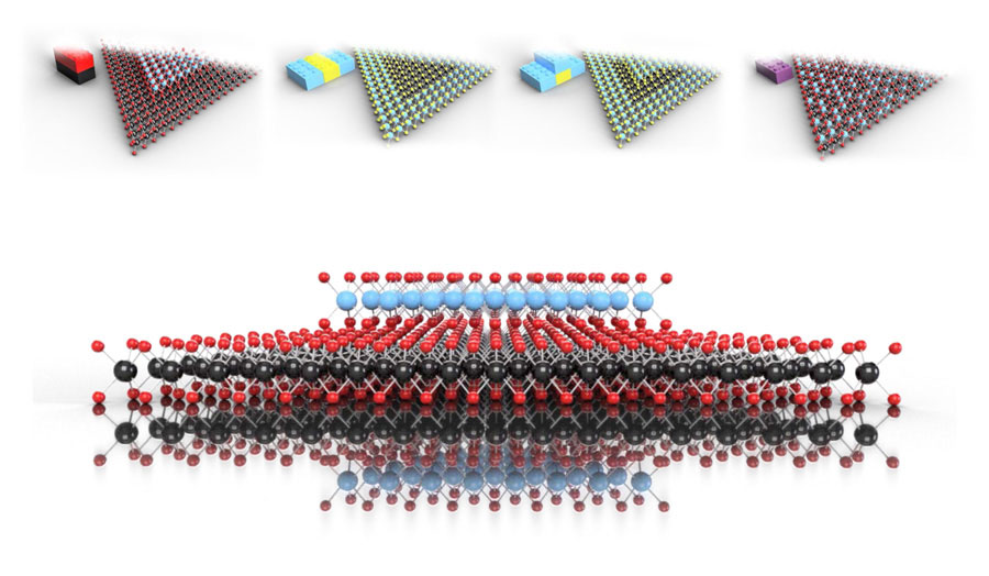
Top: Vertical MoSe2-WSe2 heterostructure, radial MoS2-WS2 heterostructure, hybrid MoS2-WS2 heterostructure and Mose2-WSe2 alloy building block representations and crystal structure models. Bottom: Vertical MoSe2-WSe2 heterostructure crystal structure model. Image: Cain, Hanson and Dravid
The unified Time-Temperature-Architecture Diagrams provide directions for the exact conditions required to generate numerous heterostructure morphologies and compositions. Using these diagrams, the researchers developed a unique library of nanostructures with physical properties of interest to physicists and materials scientists. The Northwestern University scientists are now examining the behaviors displayed by some materials in their library, like the electron flow across the stitched junctions between materials.
The researchers hope that their blueprint design will be useful for heterostructure fabrication beyond the first four materials. “Our specific diagrams would need revisions in the context of each new material, but we think that this idea is applicable and extendable to other material systems,” Cain says.
Source: American Institute of Physics