A nanostructured gate dielectric may have addressed the most significant obstacle to expanding the use of organic semiconductors for thin-film transistors. The structure, composed of a fluoropolymer layer followed by a nanolaminate made from two metal oxide materials, serves as gate dielectric and simultaneously protects the organic semiconductor — which had previously been vulnerable to…
Oxide and Semiconductor Combo Holds Promise for New Electronic Devices
Insulating oxides are oxygen containing compounds that do not conduct electricity, but can sometimes form conductive interfaces when they’re layered together precisely. The conducting electrons at the interface form a two-dimensional electron gas (2DEG) which boasts exotic quantum properties that make the system potentially useful in electronics and photonics applications. Researchers at Yale University have…
Semiconductor Lasers Surpass Conventional Silicon-Based Systems
A systematic study of a simple and general structure for on-chip semiconductor lasers by A*STAR researchers sets the scene for much broader application of integrated semiconductor lasers beyond conventional silicon-based systems (Applied Optics, “Comparison of III-V/Si on-chip lasers with etched facet reflectors”). The ability to use, manipulate and sense light is applicable to many technologies,…
Novel New Approach for Developing Semiconductors
Scientists at Tokyo Institute of Technology and their team involving researchers of JASRI, Osaka University, Nagoya Institute of Technology, and Nara Institute of Science and Technology have just developed a novel approach to determine and visualize the three-dimensional (3-D) structure of individual dopant atoms using SPring-8. The technique will improve the current understanding of the…
Breakthrough Transistors Inspired by Movement of Ions
Excitons Lured to the Dark Side

To build tomorrow’s quantum computers, some researchers are turning to dark excitons, which are bound pairs of an electron and the absence of an electron called a hole. As a promising quantum bit, or qubit, it can store information in its spin state, analogous to how a regular, classical bit stores information in its off…
Superconductivity Riddle Solved with Stripes
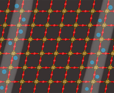
Imagine phones and laptops that never heat up or power grids that never lose energy. This is the dream of scientists working with so-called high-temperature superconductors, which can effortlessly carry electrical currents with no resistance. The first high-temperature superconducting materials, called cuprates, were discovered in the 1980s and would later be the subject of a…
New Technique Creates Eco-friendly Waterborne Semiconductor Inks
A team of researchers at Daegu Gyeongbuk Institute of Science and Technology (DGIST), led by Professor Dae Sung Chung of Energy Science and Engineering, has developed a technology to produce environmentally friendly water-borne semiconductor inks using surfactant, which is additives that mix substances of different properties and a component of soap. Polymer semiconductors are carbon…
Chipmaker to Pay $6B for Rival Company
Marvell Technology Group Ltd, a chipmaker based in Hamilton, Bermuda, has announced that it will buy smaller rival Cavium Inc., a network equipment builder in San Jose, Calif. The deal is valued at $6 billion, and is intended as a way for Marvell to expand its wireless connectivity business in the semiconductor industry and diversify…
Semiconductors Stretch Out to Become Perfect

Compressing a semiconductor to bring atoms closer together or stretching it to move them farther apart can dramatically change how electricity flows and how light is emitted. Scientists found an innovative way to compress or stretch very thin (monolayer and bilayer) films of tungsten diselenide by placing the film on different surfaces at high temperatures.…
Semiconductors Have an Aligned Interface
The electronic characteristics of an interface between two wide bandgap semiconductors are determined by researchers at King Abdullah University of Science and Technology (KAUST): an insight that will help improve the efficiency of light-emitting and high-power electronic devices. Semiconductors, such as silicon and gallium nitride, have electrical properties somewhere in between those of a conductor…
Doped-Up Semiconductors Lead to Next-Gen Electronics
Physicists at Aalto University have made a breakthrough in revising methods largely discarded 15 years ago. They have discovered a microscopic mechanism that will allow gallium nitride semiconductors to be used in electronic devices that distribute large amounts of electric power. The trick is to be able to use beryllium atoms in gallium nitride. Gallium…
Spin-Polarized Surface States in Superconductors
When it comes to entirely new, faster, more powerful computers, Majorana fermions may be the answer. These hypothetical particles can do a better job than conventional quantum bits (qubits) of light or matter. Why? Because of the spooky way Majorana fermions interact with each other at a distance. When two fermions interact, they usually dissipate…
Avoiding the Interconnect Bottleneck
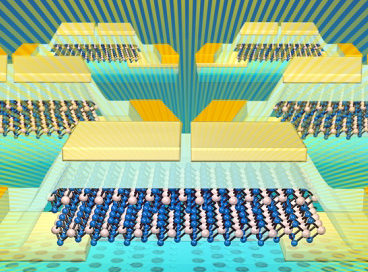
The huge increase in computing performance in recent decades has been achieved by squeezing ever more transistors into a tighter space on microchips. However, this downsizing has also meant packing the wiring within microprocessors ever more tightly together, leading to effects such as signal leakage between components, which can slow down communication between different parts…
Changing and Rearranging Semiconductors Avoids Production Problems
Super thin photovoltaic devices underpin solar technology and gains in the efficiency of their production are therefore keenly sought. King Abdullah University of Science and Technology (KAUST) researchers have combined and rearranged different semiconductors to create so-called lateral p-n heterojunctions — a simpler process they hope will transform the fabrication of solar cells, self-powered nanoelectronics,…
Breath Test Takes the Place of Blood Test
Blow into the tube, please. In the future, the procedure will not just be used by police checking for alcohol intoxication, but also for testing the condition of athletes and for people who want to lose that extra bit of weight. A sensor developed by ETH Zürich researchers makes it possible to measure when the…
Advanced Microscope Reveals Perfectly Smooth Silicon Crystals
A research collaboration between Osaka University and the Nara Institute of Science and Technology for the first time used scanning tunneling microscopy (STM) to create images of atomically flat side-surfaces of 3-D silicon crystals. This work helps semiconductor manufacturers continue to innovate while producing smaller, faster, and more energy-efficient computer chips for computers and smartphones.…
Innovative Test Improves 2-D Catalysts
Rice University researchers have taken a deep look into atom-thick catalysts that produce hydrogen to see precisely where it’s coming from. Their findings could accelerate the development of 2-D materials for energy applications as fuel cells. The Rice lab of materials scientist Jun Lou, with colleagues at Los Alamos National Laboratory, developed a technique to…
A Flexible New Platform for High-Performance Electronics
A team of University of Wisconsin-Madison engineers has created the most functional flexible transistor in the world — and with it, a fast, simple and inexpensive fabrication process that’s easily scalable to the commercial level. It’s an advance that could open the door to an increasingly interconnected world, enabling manufacturers to add “smart,” wireless capabilities…
Made-to-Order Semiconductor Band Gaps
Control is a constant challenge for materials scientists, who are always seeking the perfect material — and the perfect way of treating it — to induce exactly the right electronic or optical activity required for a given application. One key challenge to modulating activity in a semiconductor is controlling its band gap. When a material…
Applying Advanced Non-Stable Semiconductors in Nanoelectronics
A research group consisting of scientists from Tomsk Polytechnic University, Germany, and Venezuela proved vulnerability of a two-dimensional semiconductor gallium selenide in air. This discovery will allow manufacturing nanoelectronics based on gallium selenide, which has never been previously achieved by any research team in the world. The study was published in Semiconductor Science and Technology.…
Thin Semiconductor “Post-It Notes” Aid Solar Cells
Over the past half-century, scientists have shaved silicon films down to just a wisp of atoms in pursuit of smaller, faster electronics. For the next set of breakthroughs, though, they’ll need novel ways to build even tinier and more powerful devices. In a study published Sept. 20 in Nature, UChicago and Cornell University researchers describe…
Transistors Masquerade as Both Metal and Semiconductor
Modern life will be almost unthinkable without transistors. They are the ubiquitous building blocks of all electronic devices: each computer chip contains billions of them. However, as the chips become smaller and smaller, the current 3D field-electronic transistors (FETs) are reaching their efficiency limit. A research team at the Center for Artificial Low Dimensional Electronic…
Nanocrystals Assemble in Liquid
Many seashells, minerals, and semiconductor nanomaterials are made up of smaller crystals, which are assembled together like the pieces of a puzzle. Now, researchers have measured the forces that cause the crystals to assemble, revealing an orchestra of competing factors that researchers might be able to control. The work has a variety of implications in…
A New Manufacturing Process for SiC Power Devices
Researchers from North Carolina State University are rolling out a new manufacturing process and chip design for silicon carbide (SiC) power devices, which can be used to more efficiently regulate power in technologies that use electronics. The process — called PRESiCETM — was developed with support from the PowerAmerica Institute funded by the Department of…